


Scope on the C64
Content
Introduction
Supply Voltages
Supply Voltages of ASSY 250466 and earlier
RESET
Clock Signals
Clock Circuit of ASSY 250407 and earlier
AEC (Address Enable Control)
/AEC (Address Bus Multiplexor ASSY250466 and earlier)
DRAM Refresh
Data Bus
Address Bus
Chip Selects
Other CPU specific signals
Other PLA signals
Logic Chips
● U15 - I/O chip select generator
● U14 - Video Address Multiplexor
● U27 - AND gate
Color RAM
Video Signals
The Interrupts
The SID
Introduction
If all diagnostic instruments fail on a C64 repair, there is some "more advanced" instrument, that helps one to debug a faulty C64: the scope.
Sure, not everybody has one. But in case you have a scope, you still need to have a reference showing the good case. And that is, what this essay is all about.
You should understand the scape basics already, being able to set the coupling, the trigger (source and edge), the time base and the voltage per division on each channel. A dual channel scope with 20MHz or better 50MHz) is sufficient. The measurements here were conducted with a Rigol MSO4024 (upgraded to 350MHz bandwidth). Please keep in mind, that the bandwidth of your scope, the grounding etc. have an influence on how the waveforms look like.
The GND clamp of the probe is connected to the GND "frame" around the board. I have soldered so pins to it.
The status is booted up, no program execution.
Introduction
Supply Voltages
Supply Voltages of ASSY 250466 and earlier
RESET
Clock Signals
Clock Circuit of ASSY 250407 and earlier
AEC (Address Enable Control)
/AEC (Address Bus Multiplexor ASSY250466 and earlier)
DRAM Refresh
Data Bus
Address Bus
Chip Selects
Other CPU specific signals
Other PLA signals
Logic Chips
● U15 - I/O chip select generator
● U14 - Video Address Multiplexor
● U27 - AND gate
Color RAM
Video Signals
The Interrupts
The SID
Introduction
If all diagnostic instruments fail on a C64 repair, there is some "more advanced" instrument, that helps one to debug a faulty C64: the scope.
Sure, not everybody has one. But in case you have a scope, you still need to have a reference showing the good case. And that is, what this essay is all about.
You should understand the scape basics already, being able to set the coupling, the trigger (source and edge), the time base and the voltage per division on each channel. A dual channel scope with 20MHz or better 50MHz) is sufficient. The measurements here were conducted with a Rigol MSO4024 (upgraded to 350MHz bandwidth). Please keep in mind, that the bandwidth of your scope, the grounding etc. have an influence on how the waveforms look like.
The GND clamp of the probe is connected to the GND "frame" around the board. I have soldered so pins to it.
The status is booted up, no program execution.
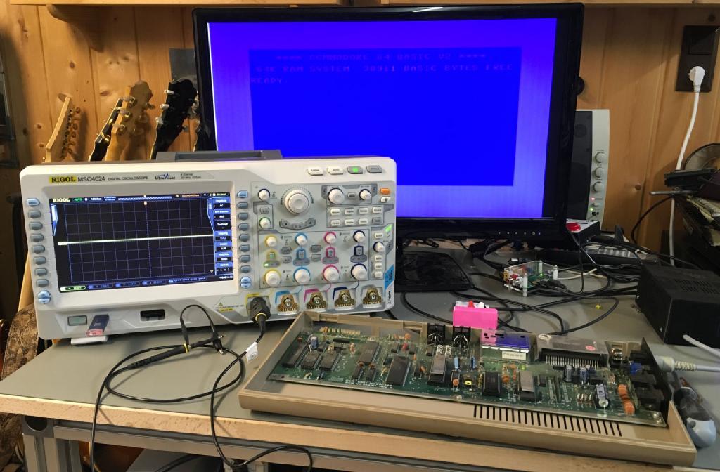
C64 with a Rigol MSO4024 scope
Finding a good ground for the probe is not so difficult in a C64. It should not be too far away from where you want to measure, because actually, the ground leads on a scope probe are evil. The bigger the area that you span with the probe and the ground lead, the more disturbance you get (= bigger the loop, the more unwanted electro-magnetic fields you will "hug" = a lot of noise).
Prior to taking all these scope screen shots, I have soldered some test pins to the solder mask free frame around the board. This might be better, than a faraway shielding enclosure.
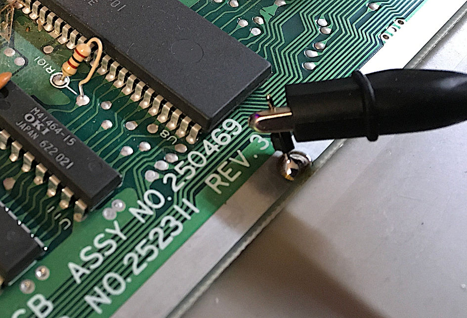
Ground pin solderd to the board
THIS IS A WORK IN PROGRESS!
Supply Voltages
There are sure more exciting signals than the supply voltages in a C64. But in case they are bad, everything is bad, so it is well worth inspecting them.
The +5VDC are probed on Pin 6 of the CPU (U6).
The settings:
Coupling = DC
Time = 100µs/DIV
Voltage = 2V/DIV
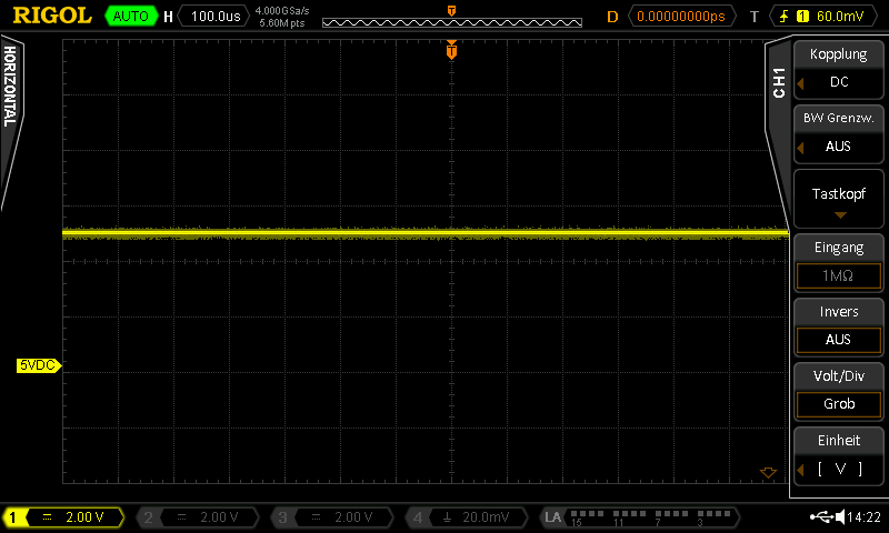
ASSY 250469, 5VDC, DC coupling
This shows, that the curve is flat (at about 5V). If not, this is critical for the function and might show a malfunction of the PSU.
There is some ripple on the 5VDC, though. The power supply (in case it is a modern one and not the original) introduces maybe 100mV or 200mV (peak-peak), which is not critical or harmful. Also, there is quite something going on in the C64, which causes further ripple.
The settings:
Coupling = AC
Time = 100µs/DIV
Voltage = 200mV/DIV
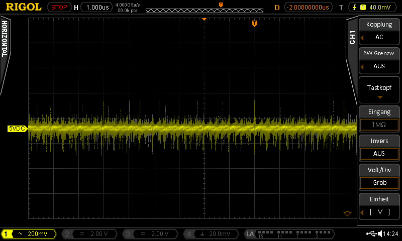
ASSY 250469, Ripple on 5VDC (AC coupling)
In ASSY 250469, there is the +9/12V, which is supplying the SID (U9 at Pin 28). This is generated from the 9VAC from the power supply.
Again, this should be smooth with a small ripple.
The settings:
Coupling = DC
Time = 1µs/DIV
Voltage = 2V/DIV
ASSY 250469, +9/12V (DC coupling)
Settings:
Coupling =AC
Time = 1µs/DIV
Voltage = 100mV/DIV
Coupling =AC
Time = 1µs/DIV
Voltage = 100mV/DIV
ASSY250469, +9/12V, Ripple
Again, the ripple is maybe 200mVpp.
Supply Voltages of ASSY 250466 and earlier
While ASSY250469 is powering the VIC-II from the 5VDC of the power supply (except the 9V), the earlier ASSY numbers generate an extra 5V ("CAN+5") and 12V from the rectified 9VAC. The obvious intention was to have a cleaner 5V for this chip, that the 5VDC ("+5"), that is powering all other digital chips, which is shows interferences.
This CAN+5 is generated with a 7805 linear voltage regulator VR2. The input voltage is measured at pin 1.
Settings:
Coupling = DC
Time = 10ms/DIV
Voltage = 2V/DIV
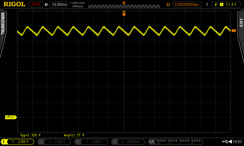
Input voltage @ VR2, pin 1
This input voltage is showing a voltage ripple of 1.3Vpp (100Hz for a 50Hz mains frequency), the ASSY250407 was not recapped. Anyways, this is probably pretty normal and is not a problem. According to the datasheet, the supply voltage rejection (SVR) of the 7805 is 68dB. That means, only 1/2500 of the input ripple will reach the output of the regulator. That is 0.5mVpp (Vpp = "Volt peak to peak"). The average input voltage is about 11.3V.
The regulator has a dropout voltage of 2V (older model maybe up to 2.5V), so it would be critical, if the input voltage drops below 7V, which is does not.
Settings:
Coupling = DC
Time = 10ms/DIV
Voltage = 2V/DIV
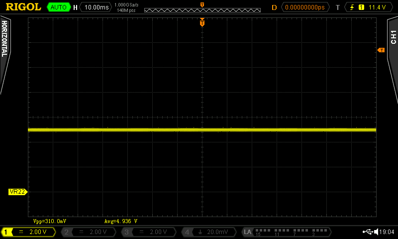
CAN+5 (V) at the ouput pin of VR2
The output voltage can be found at "Pin 2". This is in quotation marks, because the Commodore pin numbering is unusual counting 1, 3, 2 from left to right. This is not regular. All TO220 cases are actually numbered 1, 2, 3. (TO220 is the shape of the regulator cases).
CAN+5 is a straight line with some noise.
Another supply voltage generated by a voltage regulator (VR1) is the +12V. This is used to power the VIC-II and the SID (those have two supply voltages - VCC and VDD).
The input voltage of VR1 can be measured at pin 1:
Settings:
Coupling = DC
Time = 10ms/DIV
Voltage = 5V/DIV
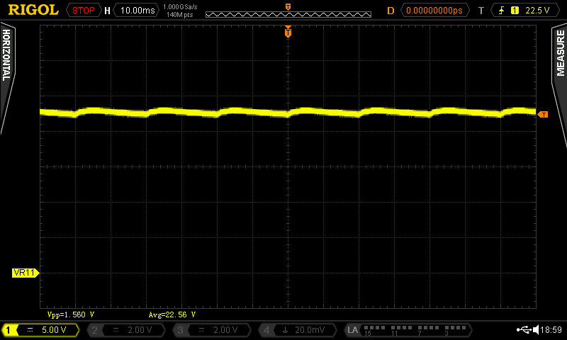
Input Voltage of VR1 at pin 1
The average voltage is 22.5V and the ripple is 1.6V. Again, no problem. This is showing a working ASSY250407.
Finally, I want to show the voltage measured at the fuse F1. It was measured between F1 and GND, which is ok, since it is related to GND, because the negative output of the bridge rectifier CR4 is connected to GND.
Settings:
Coupling = DC
Time = 10ms/DIV
Voltage = 2V/DIV
Finally, I want to show the voltage measured at the fuse F1. It was measured between F1 and GND, which is ok, since it is related to GND, because the negative output of the bridge rectifier CR4 is connected to GND.
Settings:
Coupling = DC
Time = 10ms/DIV
Voltage = 2V/DIV
9VAC measured at F1
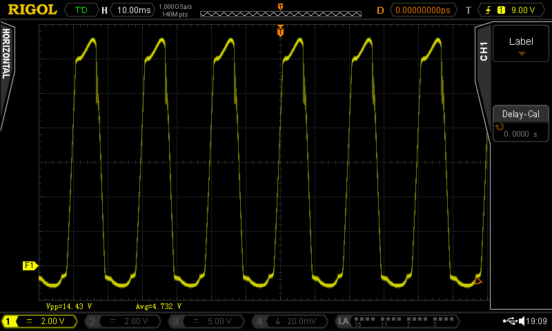
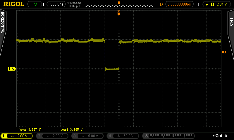
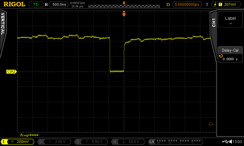
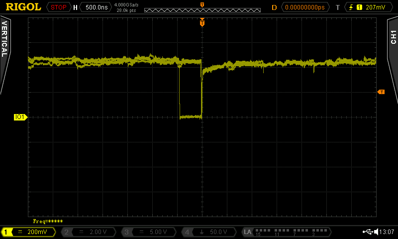
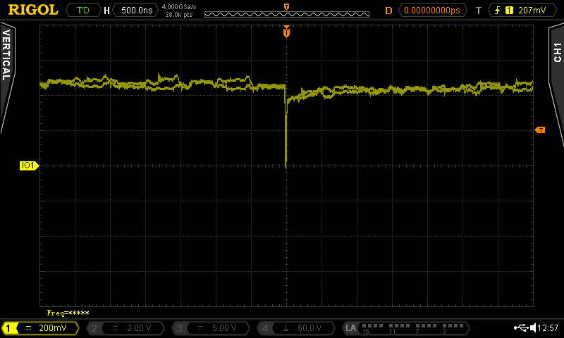
RESET
The /RESET signal is absolutely essential for the C64 to boot properly. If this is not present, the computer will most probably not work. It can be found on the CPU (U6, Pin 40).
It has to stay LOW (=close to 0V) for a couple of 100ms after switching on the power and then go HIGH.
Settings:
Coupling = DC
Time = 50ms/DIV
Voltage = 2V/DIV
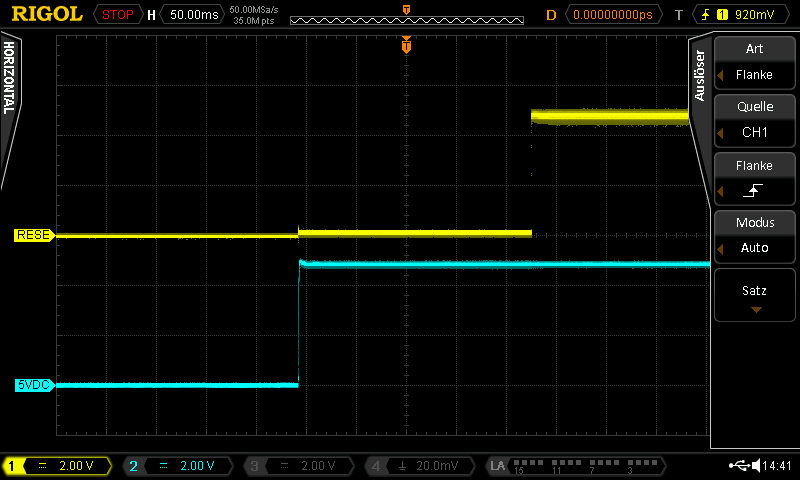
ASSY250469, /RESET signal (the 2nd (blue) channel +5VDC)
It is not really required to probe the 2nd channel, I have only done this to show the power up.
The duration of the (LOW) /RESET pulse is not very accurate, because it is generated by an R/C. For ASSY250469, U23 (a 74LS14) and some passive components (on is a 220uF e-cap) do the job. For earlier ASSYs, it id done by a 556 timer (U20).
Clock Signals
The clock signals synchronize everything in a coputer system. The are curical for the function. Besides the chrystal generator, the VIC-II is generating the PHI0 clock from the clocks provided by the chrystal generator.
Be aware, that the clock frequencies are (slightly) different for PAL and NTSC C64s.
The dot clock was probed at the VIC-II (U7, Pin 22). It is generated in the crystal generator (ASSY 250469: U20).
Settings:
Coupling = DC
Trigger= rising edge
Time = 50ns/DIV
Voltage = 2V/DIV
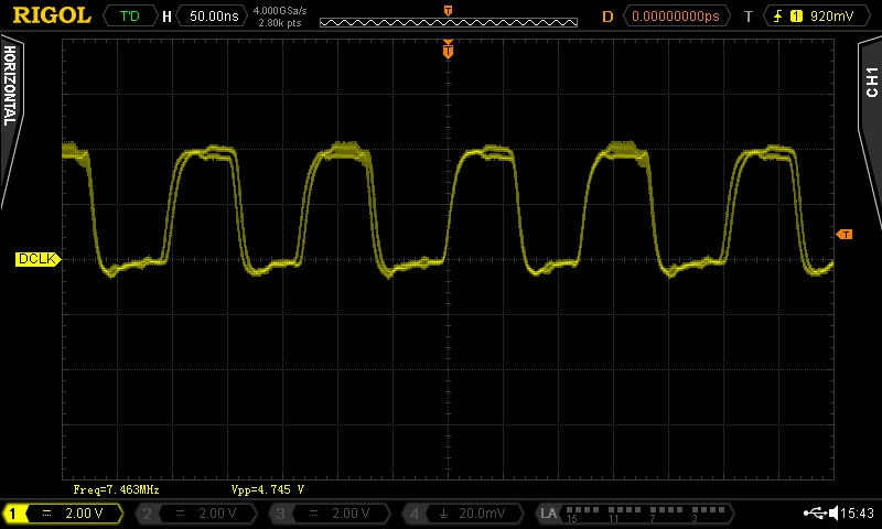
PAL ASSY 250469, Dot Clock (PAL: 7.88MHz, NTSC: 8.18MHz)
The frequencies measured with a scope are not always accurate. The signal above was not measured well or has a jitter, which is visible from the "double lines".
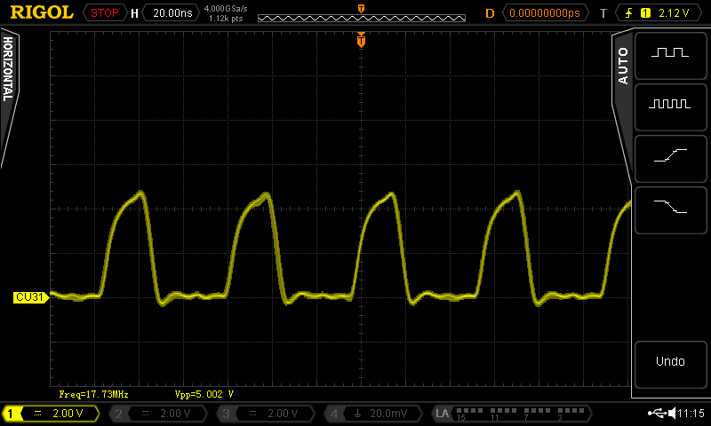
The color clock was probed at the VIC-II (U7, Pin 21). It is generated in the crystal generator (ASSY 250469: U20).
Settings:
Coupling = DC
Trigger= rising edge
Time = 20ns/DIV
Voltage = 2V/DIV
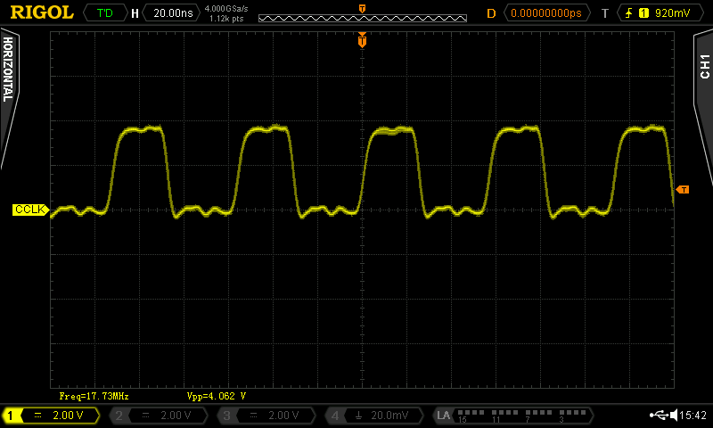
PAL ASSY 250469, Color Clock (PAL:17.73MHz, NTSC: 14.32MHz)
PHI0 is the processor clock, which is generated by the VIC-II. It is probed at the CPU (U6, Pin 1).
Settings:
Coupling = DC
Trigger= rising edge
Time = 200ns/DIV
Voltage = 2V/DIV
Settings:
Coupling = DC
Trigger= rising edge
Time = 200ns/DIV
Voltage = 2V/DIV
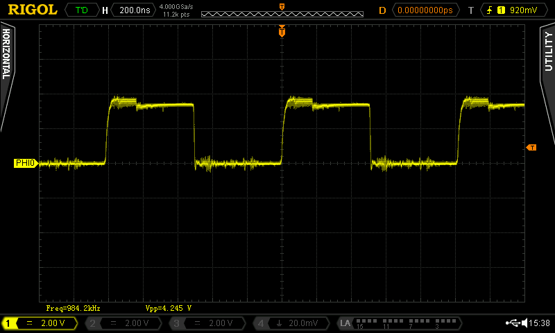
PAL ASSY250469, Phi0 (0.98MHz for PAL, NTSC: 1.02MHz)
PHI2 is the processor clock, which is generated by the CPU. It is probed at the CPU (U6, Pin 39).
Settings:
Coupling = DC
Trigger= rising edge
Time = 200ns/DIV
Voltage = 2V/DIV
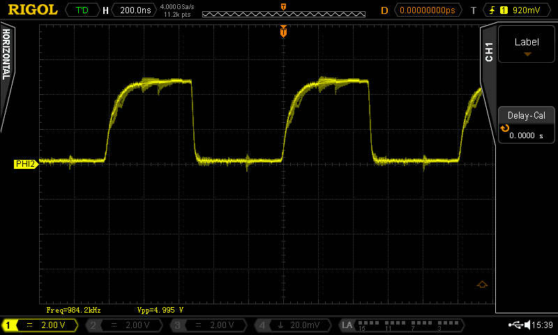
PAL ASSY250469, Pih2 (PAL: 984.2kHz, NTSC: )
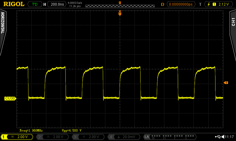
Clock Circuit of ASSY 250407 and earlier
With ASSY250425, a one chip clock generator solution was introduced, which persisted in all further ASSYs. Prior to that, the clock generation was implemented in multiple (mostly TTL) ICs. Actually, those IC form a PLL (phase locked loop) together with the VIC-II. Please check the schematics.
U31 (the half with the output Y is on Pin 10) is the crystal generator. It outputs the crystal frequency on pin 10:
Settings:
Coupling = DC
Trigger= rising edge
Time = 20ns/DIV
Voltage = 2V/DIV
Color Clock @ U31, Pin 10 (PAL: 17.73MHz, NTSC: 14,32MHz)
This color clock is feeding the respective input on VIC-II (pin 21).
U30 is a frequency devider, which is fed with the color clock and which outputs the input frequency divided by 9 (for PAL) on pin 6:
Settings:
Coupling = DC
Trigger= rising edge
Time = 200ns/DIV
Voltage = 2V/DIV
Divided color clock @ U30, Pin 6
This counter is preloaded with different values depending if wether it is an NTSC or PAL machine.
For PAL the preloaded counter value [DCBA] is [LHHH] (that is binary for 7)
For NTSC the preloaded counter value [DCBA] is [HLLH] (that is binary for 9)
The counter counts up from 7 (or 9 for NTSC) to 16, which results in 9 (or 7) clock cycles until overflow.
So, for PAL, the output clock is 17.734472 MHz / 9 = 1.956 MHz, which is twice the system clock.
For NTSC, the resulting clock on pin 6 is 14.31818 MHz / 7 = 2.045 MHz, which is also twice the (NTSC) system clock.
The D-Flipflop U29 (with Q on pin 9) is a divider by two. The resulting clock on pin 9 is 0.978MHz for PAL and 1.0225MHz for NTSC.
Settings:
Coupling = DC
Trigger= rising edge
Time = 200ns/DIV
Voltage = 2V/DIV
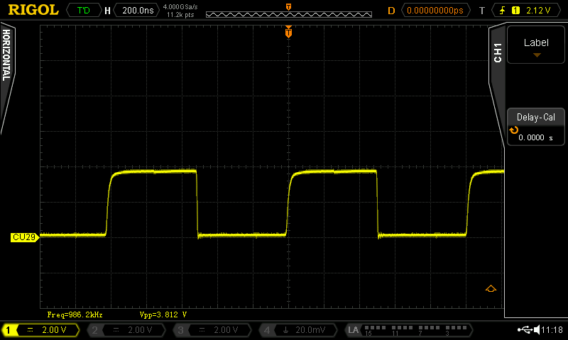
System Clock @ U29, Pin 9
The VIC-II generates the system clock PHI0 from the dot clock (it is just a devided by 8). The dot clock is generated by U31. This is a voltage-controlled oscillator, in this case. The frequency is generated with R101 and C86, which is not very accurate and not necessarily in phase with the system clock.
But here comes the PLL thing! That is "phase locked loop", like I mentioned before. This creates a fix frequency and phase relation of all those clocks.
The frequency of U31 is controlled with the analog voltage on "FREQ CONT" pin 2 (of U31). And this analog voltage is generated by the phase detector U32.
This has two clock inputs. One is pin 1, which is fed by the 0.978MHz (1.0225MHz for NTSC) from U29, pin 9 and the other clock input is U32, pin 3. Here, the PHI0 from the VIC is connected.
Depending on the phase relation between both clocks, a voltage is generated on U32, Pin 10 (and 5). This voltage is filtered with R19, R16, R17, C85, Q7 and the final stage of U32. The output is pin 8, which is the frequency control input of U31 (pin 2). The frequency of U31 is varied as long as PHI0 and the frequency from the crystal oscillator are exactly in phase. This is, where that thing forms a loop.
Now let's have a look at all those voltages and frequencies.
Settings:
Coupling = DC
Trigger= rising edge, CH1
Time = 500ns/DIV
Voltage = 2V/DIV
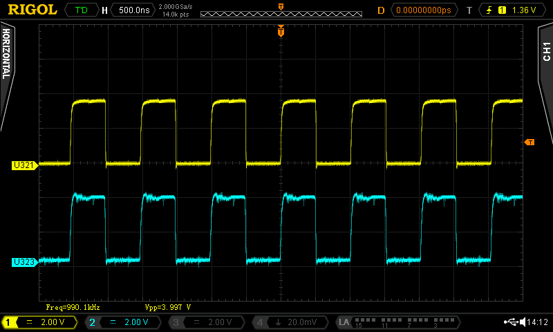
Input signals of the phase detector U32.
The input signals on pin 1 (yellow) and pin 3 (blue) must have the same frequency, they are exactly in phase. This is the evidence of a working clock circuit. If this is not the case, something is wrong with the clock circuit of U31/U32.
This is the output voltage on U32, Pin 10:
Settings:
Coupling = DC
Trigger= rising edge
Time = 500ns/DIV
Voltage = 1V/DIV
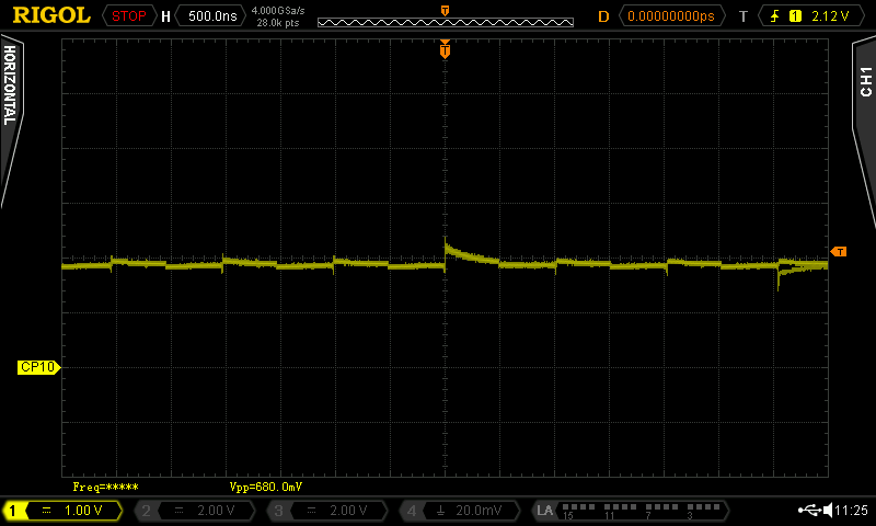
U32, Pin 10
This is an analog signal, the voltage is about 2V, which may vary, depending on the R101/C86 at U31. It is still a bit fluttering and it needs some filtering. The filtered signal appears on U32, pin 9:
Settings:
Coupling = DC
Trigger= rising edge
Time = 500ns/DIV
Voltage = 1V/DIV
Settings:
Coupling = DC
Trigger= rising edge
Time = 500ns/DIV
Voltage = 1V/DIV
U32, Pin 9
This is a flat voltage of about 1.5V.
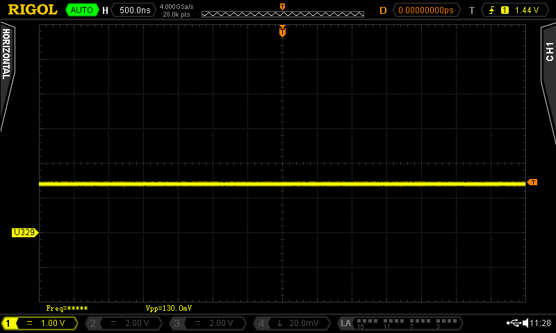
The signal, which is controlling the dot clock generator (U31, R101, C86) at Pin 2 is generated at U32, pin 8.
Settings:
Coupling = DC
Trigger= rising edge
Time = 500ns/DIV
Voltage = 1V/DIV
U32, Pin 8
This is a flat voltage of about 1.5V. This value is not necessarily the same in every ASSY 250407, since it depends on the values of C86 and R101, which both have tolerances and the thresholds in U31.
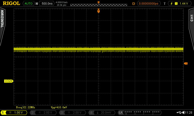
AEC: Address Enable Control
The AEC signal is generated by the VIC-2 chip. It determines, that either the VIC or the CPU can access the system busses. This is another important signal, that is required for a working C64 (sure, everything is required, but this signal is a show stopper).
While AEC is HIGH, the CPU can access the RAM, while it is LOW, the VIC-2 accesses the RAM (e.g. for refreshing the DRAM). It also controls, who can access the color RAM.
The AEC signal can be probed in several locations, here it was U3, Pin4.
Settings:
Coupling = DC
Trigger= rising edge
Time = 500ns/DIV
Voltage = 2V/DIV
ASSY 250469 (PAL) - AEC
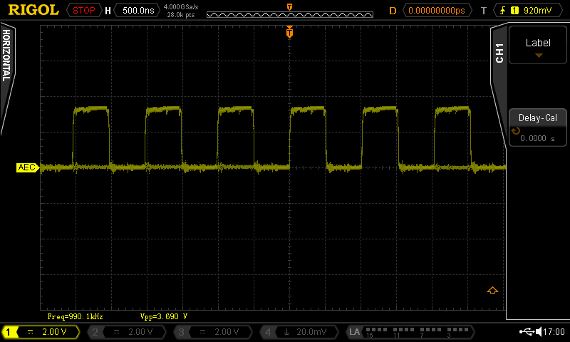
/AEC: Controlling the Address Bus Multiplexor (ASSY 250466 and before)
The DRAM has a multiplexed address bus. This means, that either the low or the high byte of the address is present at the DRAM address pins MA0...MA7. Sure, 64k addresses require 16 address bits.
The multiplexing is done by U13 and U25. The selection, which part of the address, A0...7 or A8...15 is present at the DRAM is done by the signal /CAS (column address select). LOW is selecting A8..15, HIGH A0..7. To allow the VIC-II accessing the DRAM, the multiplexors are switched to "high Impedance" (HiZ). That actually means, the outputs of U13 and U25 are switched off (not LOW). While this happens, AEC is LOW (like mentioned before). U8 is the inverter, that outputs /AEC (at pin 4).
Settings:
Coupling = DC
Trigger= rising edge
Time = 500ns/DIV
Voltage = 2V/DIV
/AEC @ U8, pin 4
This signal needs to be checked in case of a black screen. U8 also drives the (serial) IEC bus and is a part that is more likely to fail. In case U13 and U25 are MOS branded ICs, they might be replaced by "proper" 74LS257.
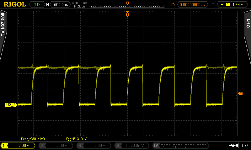
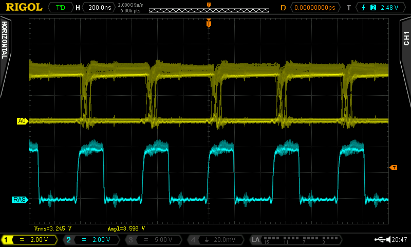
The /RAS signal selects between the low and high byte on the DRAM address multiplexor (pin 1 of U13 and U25). The /AEC is the output enable for the address multiplexors (pin 15, U13 and U25)
Settings:
Coupling = DC
Trigger= rising edge/CH2 (RAS)
Time = 200ns/DIV
Voltage = 2V/DIV

/AEC (yellow) and /RAS (blue)
/RAS is a pulse chain, /AEC can be LOW or HIGH.
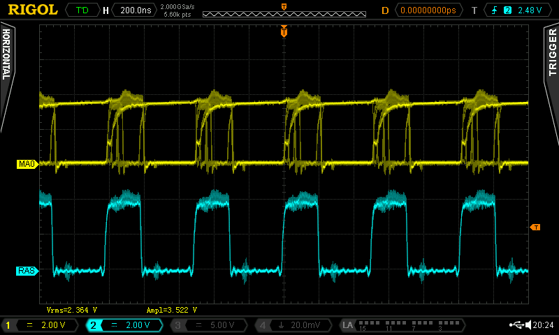
Multiplexed address (MA0) and /RAS
The multiplexed addresses do noi necessarily change levels synchronous with /RAS. That is matter of the addresses A0..15 are not perfectly aligned to /RAS, either.
A0 (U25, Pin 3) and /RAS (U25, Pin 1)
DRAM Refresh Signals
The VIC-2 refreshes the content of the DRAM periodically. A DRAM cell (bit) is actually a small capacitor, that holds the information (0 or 1). This capacitor has to be recharged after a short time, so it can keep the information).
The signals are probed at the 4x64k DRAMs of ASSY250469. /RAS is Pin 5, /CAS is Pin 16 of U10 and U11.
Settings:
Coupling = DC
Trigger= rising edge
Time = 500ns/DIV
Voltage = 2V/DIV
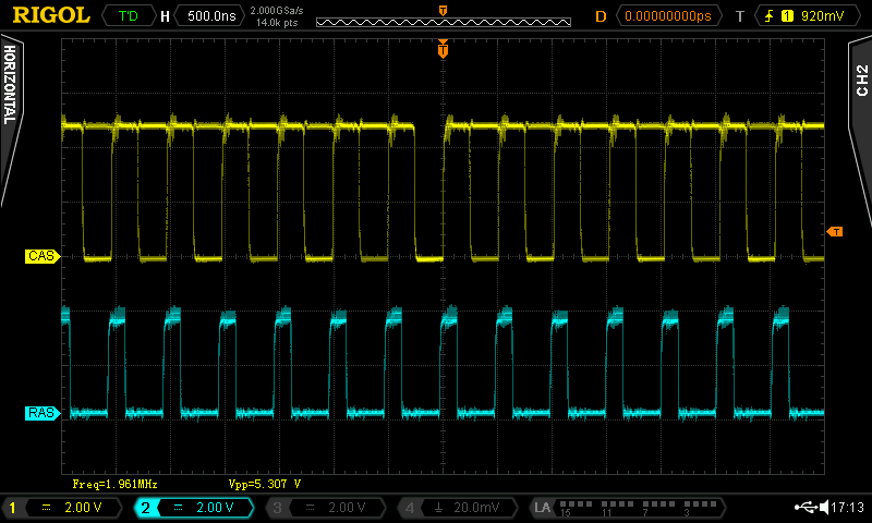
ASSY 250469: CAS (yellow) and RAS (blue)
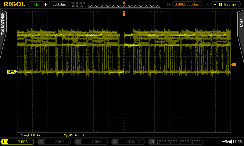
Data Bus
The Data Bus is the highway, on which the information is being transported from the CPU to the RAM, the ROM and other peripherals and back. There is always activity on every bit of the data bus. It is not a steady display, but it is pretty random. Since the sources of data are different (data might be issued by the CPU or might be read from one of the various peripherals), the levels are slightly different. Nevertheless, the LOW and the HIGH levels should not exceed or fall below certain levels. A 2V level is bad. A 3.5V to 5V level is still good.
The data bus can be probed at the CPU (U6, D[0..7] is Pin 37...30).
Settings:
Coupling = DC
Trigger= rising edge
Time = 500ns/DIV
Voltage = 2V/DIV
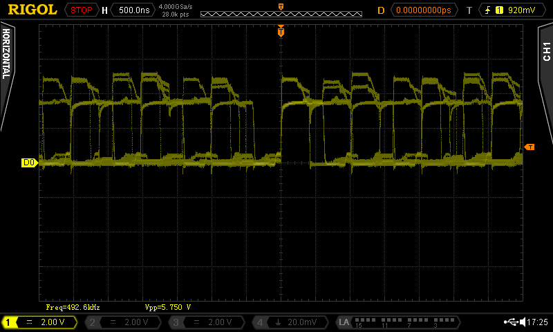
ASSY250469: Data Bus D0
D0 is representing all other data bus lines.
Address Bus
The Address Bus signals are issued by the CPU (A0...15) and the VIC-II (MA0...7). Both chips control the busses at certain times. The big PLA of ASSY250469 also accessed MA0...7, on earlier ASSYs, this job is also done by multiplexers (U13 and U25).
The Bits A0...15 can be probed at the CPU (U6, Pin 7...20, 22...23).
Settings:
Coupling = DC
Trigger= rising edge
Time = 500ns/DIV
Voltage = 2V/DIV
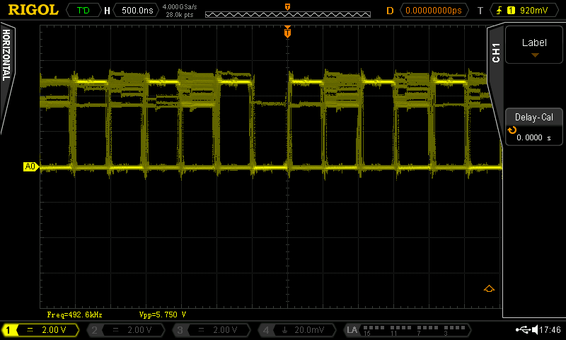
ASSY250469: Address Bit A0
ASSY250469: Address Bit A15
The lower address bits rather look like A0, the higher are a bit less active and look like A15. Both is ok.
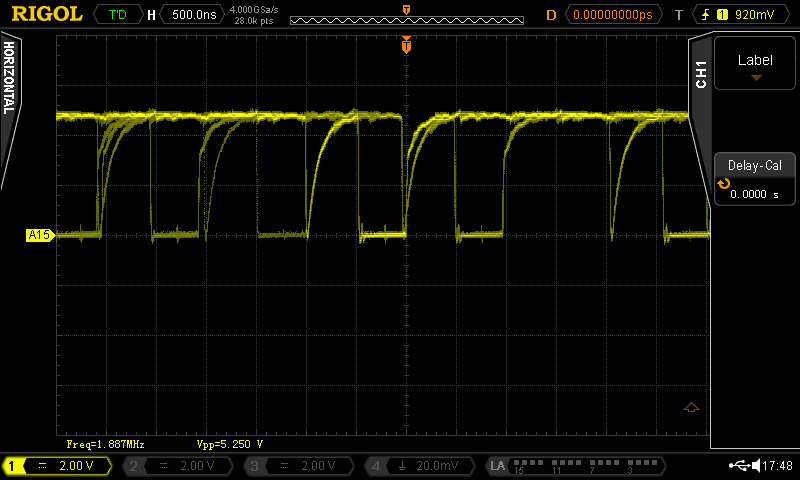
The MA0-7 (multiplexed) address bits are used to access the DRAM. They can be measured there. On the ASSY250469 4x64k DRAM, they can be located on U10 and U11.
The MA0-7 (multiplexed) address bits are used to access the DRAM. They can be measured there. On the ASSY250469 4x64k DRAM, they can be located on U10 and U11.
ASSY250469: MA0
Again, the display is not steady, but the levels should not be tied to one level only and they should be clearly LOW or HIGH (this can vary a bit, 4V levels are ok, 2V levels are not ok).
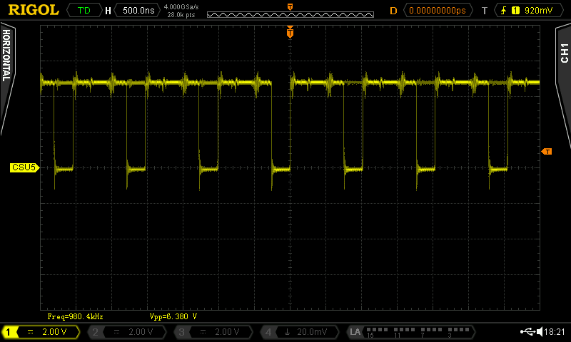
Chip Select Signals
The CPU issues the absolute address of the chip, that it wants to access, those chips do not have an inherent address, though. They know, that "they are meant" by a chip select signals, that solely addresses them. The chip, that translates the addresses to the chip selects is the PLA. The chip selects are "active low", which means, that it is HIGH while being inactive (most of the time) and go LOW, when the particular chip is addressed.
In case the address bus seems to be working (see the previous chapter), but the chips are not addressed, the PLA might be the culprit (or a dead chip, that ties the signals to a certain level).
Some of the chip selects are issued all the time, when the boot screen is displayed. The BASIC and Kernal (ASSY250469: U4) are then permanently accessed. The chip select is at pin 22. In earlier ASSYs, BASIC and Kernal are on different chips (U3 and U4). These chip selects can be found on pin 20 (each).
Settings (for all Chip Selects):
Coupling = DC
Trigger= rising edge
Time = 500ns/DIV
Voltage = 2V/DIV
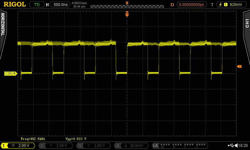
ASSY 250469: Chip select U4 (BASIC & Kernal ROM)
The character ROM (U5) is permanently accessed by the VIC-22. The chip select is located at Pin 20.
ASSY 250469: Chip select U5 (Character ROM)
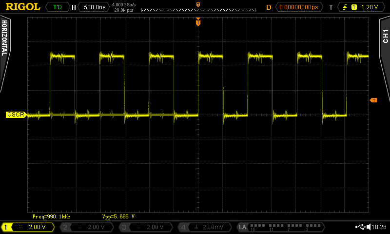
There is also a permanent activity on U1, this CIA is responsible for the keyboard (scan). The chip select is on Pin 23.
ASSY 250469 Chip select U1 (CIA1 Keyboard scan)
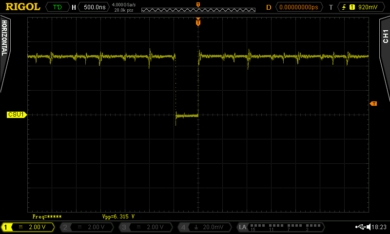
The last chip with permanent activity is U19, the color RAM, which is permanently accessed by the VIC-II.CS is on Pin 8.
ASSY 250469: Chip select U19 (color RAM)
The chip selects of the other peripherals, like CIA2 (U2, Pin 23), SID (U9, Pin 8) and VIC (U7, Pin 10) are inactive, while the C64 is idling on the boot screen. They require a certain software to be active. A Diagnostic Rev. 586220 will access those chips, while they are tested (most of the time, they are still not tested). Setting the scope to "single shot" will be able to detect such a CS-pulse. You need to be patient for that. The result will probably look like the CS of U1.
Other CPU specific signals
The CPU (U7) has an input for AEC (Pin 5). The signal here is called CAEC, which is not the pure AEC signal as issued by the VIC, but it is combined with the DMA signal, which is produced by some fancy cartridges (like the Ultimate II+) on the expansion port. CAEC is output of U27 (Pin 3).
Settings:
Coupling = DC
Trigger= rising edge
Time = 500ns/DIV
Voltage = 2V/DIV
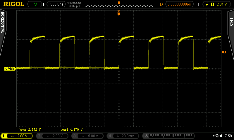
CPU signal CAEC
Since DMA is HIGH while not in use, the CAEC should look like the AEC signal.
The R/W signal is used for distinguishing between a read and a write access by the CPU. While a write access, this signal is LOW. It can be probed on U7, Pin 38, but is is also connected to several other chips. It is not a beautiful looking signal.
Settings:
Coupling = DC
Trigger= rising edge
Time = 500ns/DIV
Voltage = 2V/DIV
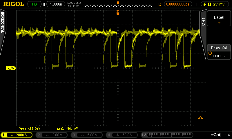
CPU Signal R/W
The RDY signal is equal to the BA signal, which is produced by the VIC-II. At least as long as DMA is not active (=HIGH). It is produced by the AND Gate U27 (Pin 11) and can be probed at teh CPU (U7, Pin 2).
Settings:
Coupling = DC
Trigger= rising edge
Time = 20us/DIV
Voltage = 2V/DIV
Settings:
Coupling = DC
Trigger= rising edge
Time = 20us/DIV
Voltage = 2V/DIV
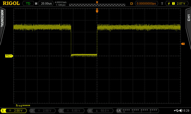
RDY at U7, Pin 2
RDY is a periodic signal (about every 512µs).
Settings:
Coupling = DC
Trigger= rising edge
Time = 100us/DIV
Voltage = 2V/DIV
Settings:
Coupling = DC
Trigger= rising edge
Time = 100us/DIV
Voltage = 2V/DIV
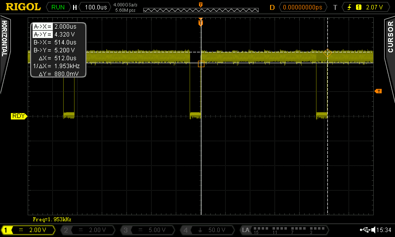
RDY at U7, Pin 2
Other PLA output signals
The PLA is generating a couple of Chip Select signals. Some are described before. Some are not always active, at least now while the C64 is idling at the read prompt. Those usually require some "special conditions" to get active. The dead test cartridge and the diagnostic rev. 586220 cartridge should be available to most of those, who probe the C64 with a scope. They are useful for getting those chip selects busy.
The Diagnostic cartridge is running from an EPROM (on a cartridge PCB), which is mapped to the ROML chip select on the expansion port. While this cartridge is running, ROML is active most of the time (except a certain RAM test routine). It can be probled at the PLA (U17, Pin 11) on the DIP28 PLA of the ASSYs prior to ASSY 250469. Or the Super PLA (U8, Pin 44).
Settings:
Coupling = DC
Trigger= rising edge
Time = 500ns/DIV
Voltage = 2V/DIV
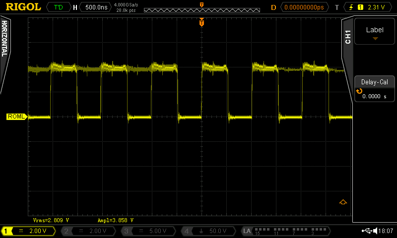
ROML while Diagnostic Rev. 586220 is running
The Dead Test 781220 is running from an EPROM mapped to the ROMH chip select on the Expansion Port. The ROMH should be active all the time. It can eb probed at the PLA (U17, Pin 10) or the Super PLA (U8, Pin 50) of ASSY250469.
Settings:
Coupling = DC
Trigger= rising edge
Time = 500ns/DIV
Voltage = 2V/DIV
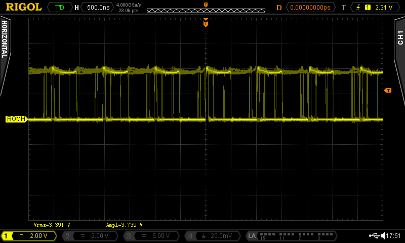
ROMH while Dead Test Rev. 781220 is running
The I/O signal is permanently active, even at the READY prompt. This is, because the chip select for CIA 1 is generated from it (in U15), due to the keyboard scan. It can be probed at PLA (U17, Pin 12). I/O cannot be found on ASSY250469, since it is an internal signal inside the Super PLA.
Settings:
Coupling = DC
Trigger= rising edge
Time = 500ns/DIV
Voltage = 2V/DIV
I/O while boot screen
Logic Chips
Many of the ligic chips can onle be found on the boards prior to ASSY250469, where their function was miograted to the Super PLA
U15 - I/O-Chip select generator
U15 is a multiplexor (74LS139), which generates the chip selects for the I/O address area.
This is the VIC, SID, Color RAM, CIA1, CIA2, I/O1 and I/O2 (the latter two are chip selects for expansion cartridges). It was merged into the Super PLA of ASSY250469.
CIA1 is always active (on the READY. Prompt), since it is responsible for the keyboard scan. The screen shot can be found here.
To activate CIA2, a short BASIC program has to be running, which is accessing CIA2.
10 PRINT PEEK(56576) : GOTO 10
The Chipselect for CIA2 can be probed at U15, Pin 11.
Settings:
Coupling = DC
Trigger= rising edge
Time = 500ns/DIV
Voltage = 2V/DIV
CIA2 at U15, Pin 11
The signal I/O1 is a chip select signal for a cartridge in the expansion port (in case it is required). It is not active on the READY. Prompt, thus, it requires a short BASIC program to get active.
10 PRINT PEEK(56832) : GOTO 10
The Chipselect for CIA2 can be probed at U15, Pin 10.
Settings:
Coupling = DC
Trigger= rising edge
Time = 500ns/DIV
Voltage = 2V/DIV
I/O1 at U15, Pin 10
The picture before shows there is a glitch - a short low pulse while the actual chip select is 500ns (one division) wide. This glitch is matter of the non synchronous logic and can be found even while I/O1 is not accessed.
The glitch at U15, Pin 10 (I/O1), while I/O1 is inactive
The signal I/O2 is a chip select signal for a cartridge in the expansion port (in case it is required). It is not active on the READY. Prompt, thus, it requires a short BASIC program to get active.
10 PRINT PEEK(57088) : GOTO 10
The Chipselect for I/O2 can be probed at U15, Pin 9.
Settings:
Coupling = DC
Trigger= rising edge
Time = 500ns/DIV
Voltage = 2V/DIV
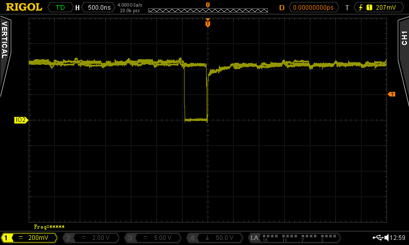
I/O2 at U15, Pin 9
There is this glitch again, so this is, how it looks like while not being active:
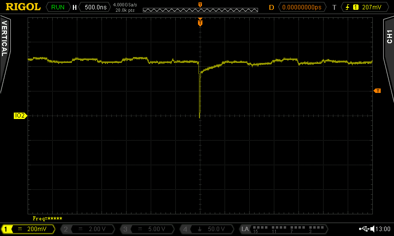
The glitch at U15, Pin 9 (I/O2), while I/O2 is inactive
U14 - Video Address Multiplexor
U14 is a video address multiplexor, a 74LS258. Its function was merged into the Super PLA of ASSY250469.
Settings:
Coupling = DC
Trigger= rising edge
Time = 500ns/DIV
Voltage = 2V/DIV
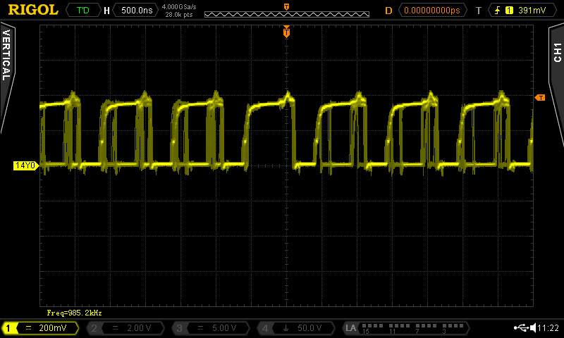
U14, Pin 4: Y0
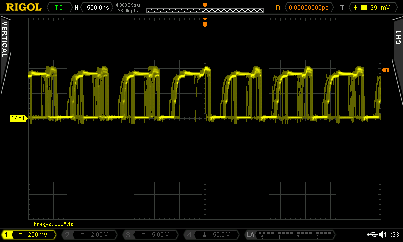
U14, Pin 7: Y1
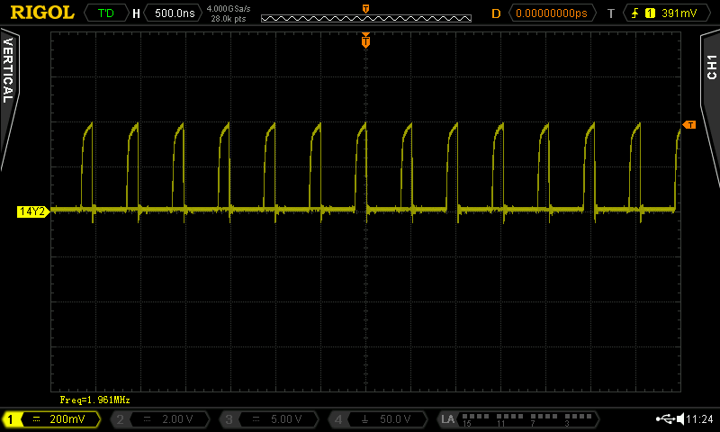
U14, Pin 12: Y2
U14, Pin 9: Y3
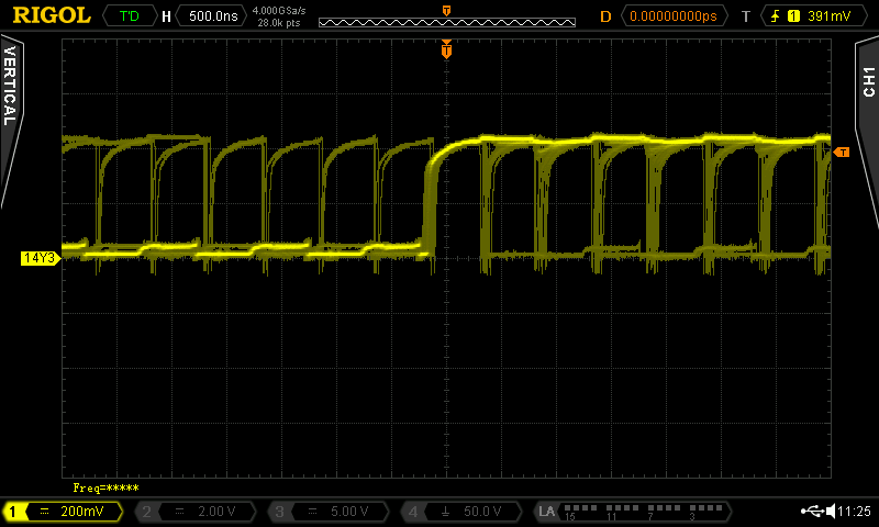
U27 - AND Gate
This AND gate (74LS08) plays an important role, since it produces many system relevant signals. Its functionality was migrated to other logic chips in ASSY250469.
Some are mentioned elswhere on this page. Those are:
● CAEC (U27, Pin 3)
● RDY (U27, Pin 11)
● Chip Select for the Color RAM (U27, Pin 6)
The Time of Day Clock (TOD) depends on the mains frequency. It is either 50Hz or 60Hz. The Input (U27, Pin 9) looks "analogish", so U27 forms this signal.
Settings:
Coupling = DC
Trigger= rising edge
Time = 5ms/DIV
Voltage = 2V/DIV
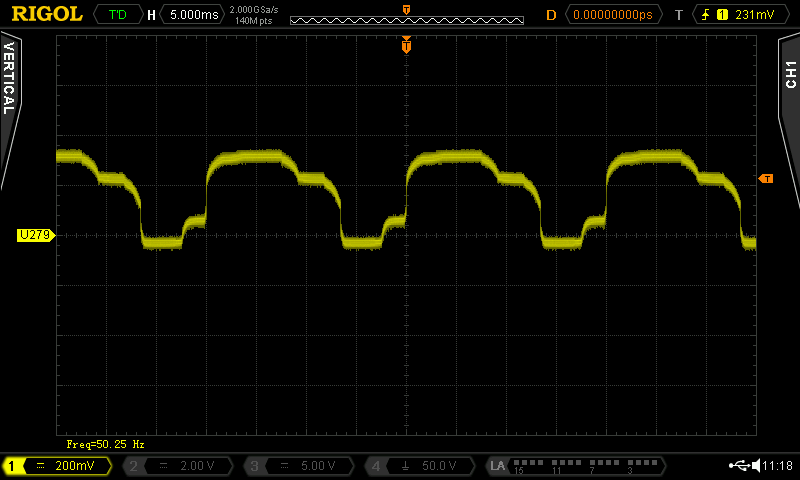
U27, Pin 9
The output signal (Pin 8) looks digital, though.
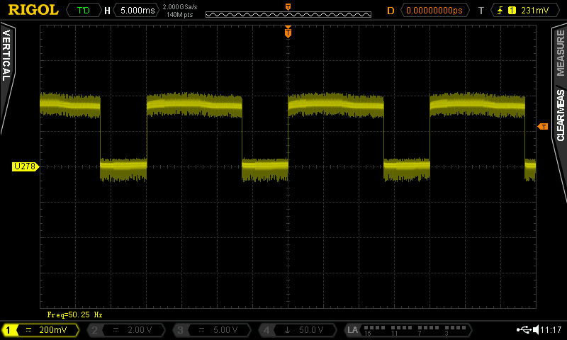
U27, Pin 8
Color RAM
The Color RAM U6 (U19 on ASSY 250469 prior to Rev. B) is a 4x512Byte static RAM, it does not require any refresh (like the regular 64k DRAM). It is permanently accessed by the VIC-II and can be accessed by the CPU as well.
The Chip Select is produced by U27 (Pin 6).
Settings:
Coupling = DC
Trigger= rising edge
Time = 500ns/DIV
Voltage = 2V/DIV
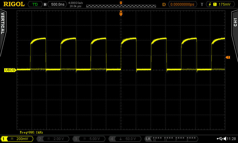
CS of Color RAM (U6, Pin 8)
The Write Enable WE (U6, Pin 10) occures periodically while the READY. prompt. It is produced in the PLA (U17, Pin 13).
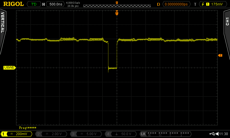
WE @ U6, Pin 10
The Video Signals
In case there is no video being displayed on your monitor, it might be useful to check the output of the VIC-II and the RF modulator to exclude a broken video cable or a not working display.
The settings for the video signals are:
Coupling = DC
Trigger= rising edge
Time = 10us/DIV
Voltage = 500mV/DIV
Please keep in mind:
1. The video signals are analog signals (no LOW and HIGH levels here)
2. The signals depend on the content of the display. Other colors (other kernals) might have different signal forms. This is the regular boot screen in light blue/blue.
3. It is not very easy to get a steady signal here. It might require fiddling with the trigger level.
The SLUM signal is generated on the VIC-II. It can be found at U7, Pin 15. It is the LUMA signal, before the processing in the RF-modulator. The RF-Modulator does have an influence on the signal, even if no TV (RF) output is required.
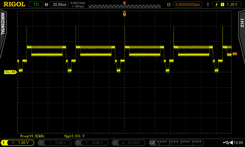
The SLUM signal of the VIC-II for light blue border and blue background
Here, every of those "cycles" and a scan line on the display. First comes the HSYNC pulse, then come the boarder (brighter than the background), the background (the voltage is lower). the scan lines on top and bottom of the screen are light blue. This is, why there is a 2nd level (line) for light blue.
The COLOR signal (from the VIC-II) can be found at U7, Pin 14.
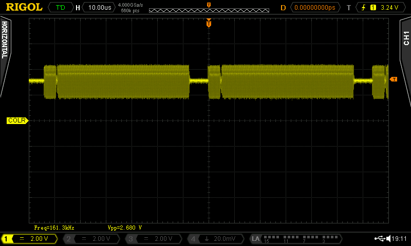
The COLOR signal is generated by the VIC-II
This is the COLOR (Burst). It is not easy to get it steady on the scope display.
The Composite Video signal is generated in the RF modulator and can be probed at the ferrite bead FB2.
The Composite Video signal is generated in the RF modulator and can be probed at the ferrite bead FB2.
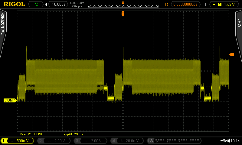
The Composite Video signal. It contains both, the luminance and the chrominance (color) information
The (S-Video) Luminance is generated in the RF modulator and can be probed at FB3.
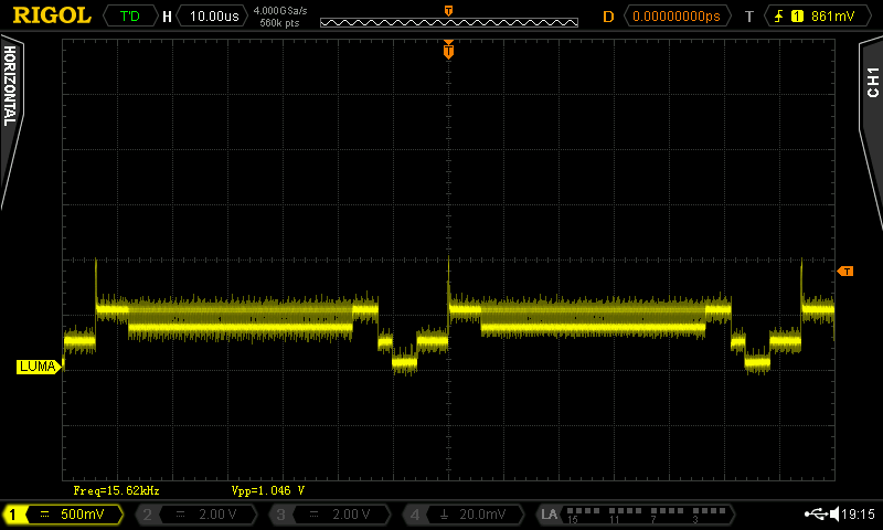
Luminance
The (S-Video) Chrominance is also generated in the RF modulator and can be probed at FB4.
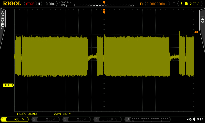
Chrominance
The Interrupts
The interrupts are signals that let the CPU branch from normal execution to special interrupt routines. They are generated by the peripheral chips CIA1, VIC-II or a cartridge in the extension port.
/IRQ can be probed at U6, Pin 3.
The settings:
Coupling = DC
Trigger= rising edge
Time = 2ms/DIV
Voltage = 2V/DIV
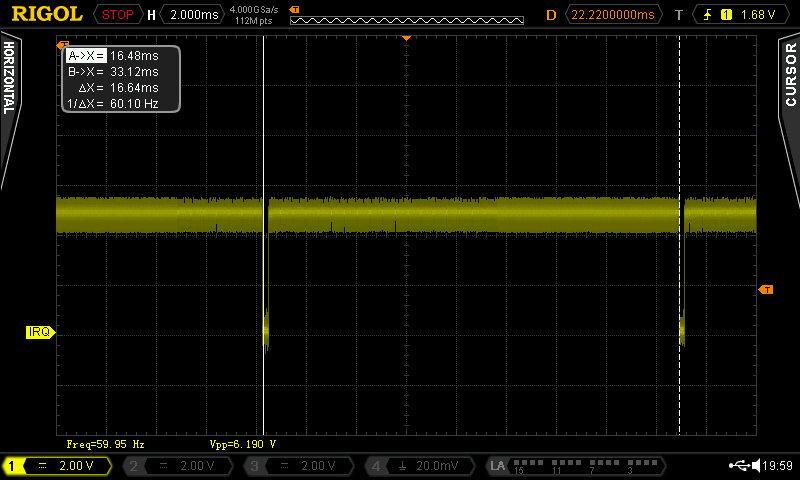
/IRQ
/IRQ is active LOW. A pulse is issued by the CIA1 about every 1/60 second. I assume, that this is the tick for the TI (1/60s) counter.
/NMI can be probed at U6, Pin 4. It is usually HIGH (idle).
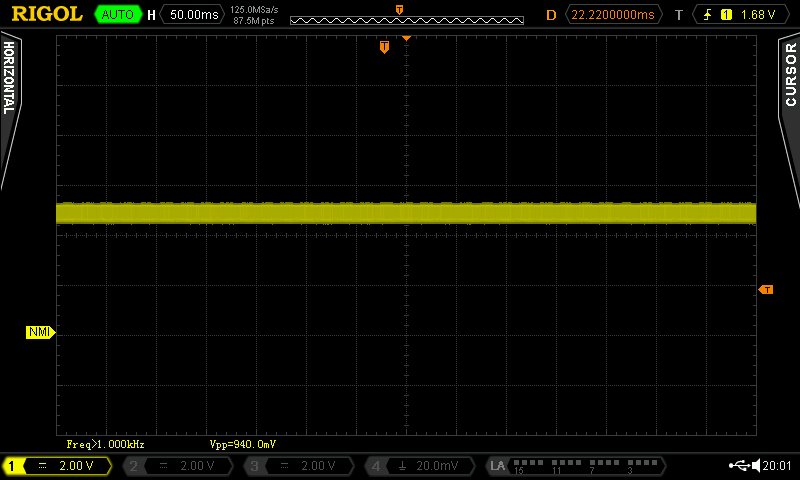
/NMI
SID
The SID (sound chip U9) is an interesting device to inspect with a scope, since it involves analog as well as digital signals.
The following measurements were carried out on an MOS8580R5 of ASSY250469.
Two potentiometers can be connected per control port. Those are the POTAX and POTAY on Port 1 and POTBX and POTBY on Port 2. The SID only has two potentiometer inputs (POTX and POTY), so an analog multiplexor is used to select one port. This is U18, a 4066 (analog switch).
The potentiometers are connected between the respective input and the +5V of the control port.
CIA1 (U1) is responsible for the selection. PA7 = HIGH (COL7) selects POTBX and POTBY (Port 2) and PA6 = HIGH (COL6) selects POTAX and POTAY (Port 1).
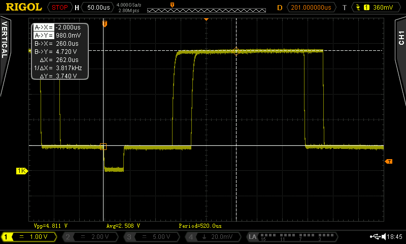
A measurement cycle looks like this:
1. the measurement capacitors (C80 for POTX and C81 for POTY) are discharged by the SID for 256 clock cycles (that is 256/978kHz = 262µs for PAL and 256/1022.5kHz = 250µs for NTSC).
2. the capacitors are charged via the potentiometers until the threshold voltage is reached. The charging time is counted in clock cycles.
3. this measurement is repeated every 512 cycles.
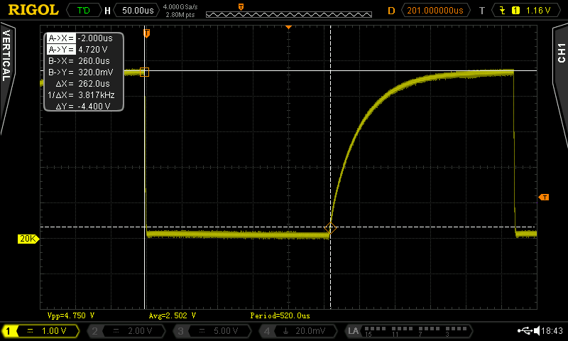
Measurement cycle for a 20k resistor
This measurement depends on the actual value of the capacitors. Typical tolerances for those are +/-10%. It also depends on the threshold voltage, which is typical VCC/2.
The previous image shows the discharge phase (flat line), which is (delta X) 262µs. Next is the capacitor charging curve. The cycle duration (period) is 520µs. The paddle value is 22. Due to the high tolerances, those are typical for a particular C64. A deviation does not indicate malfunction.
The previous image shows the discharge phase (flat line), which is (delta X) 262µs. Next is the capacitor charging curve. The cycle duration (period) is 520µs. The paddle value is 22. Due to the high tolerances, those are typical for a particular C64. A deviation does not indicate malfunction.
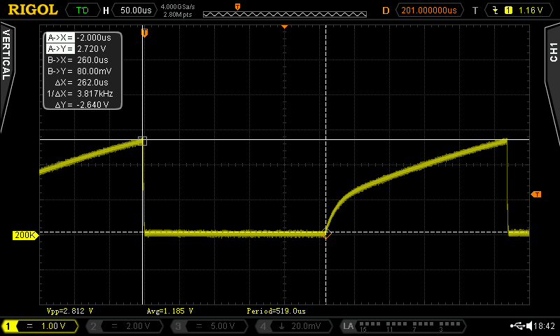
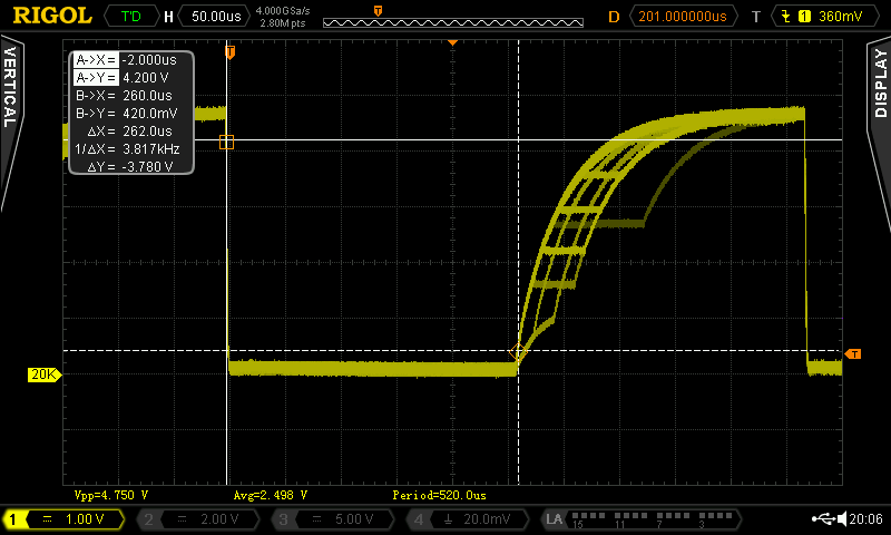
Measurement cycle for a 200k resistor
The same measurement looks different for a 200k resistor. The charging curve is flatter, since less current through the resistor takes much longer to charge the capacitor. The reading for this resistor is 149.
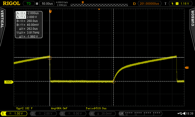
Measurement cycle for a 390k resistor
The reading for 390k is 255 on the particular C64. It is obvious, that there are settings on the 470k pot (above 390k) that are all read 255, about 45° of the paddle positions are without any effect, which is normal. On a paddle the maximum resistance is reached, the completely turned counter clockwise, and the minimum resistance (close to 0 ohms) is reached in the clockwise direction.
While the potentiometer is set to a value below about 15kohms the curve gets irregular.
While the potentiometer is set to a value below about 15kohms the curve gets irregular.
Measurement cycle for a 1k resistor
The voltage when discharged is higher than before and interference pulses occur. The readings are low, but still stable.
At higher values of the potentiometer, glitches occur. This can be made visible with a longer persistence time of the scope.
Glitches in the measurement cycle
Those glitches happen while the keyboard scan. COL6 = LOW switches the Port 1 pots off.
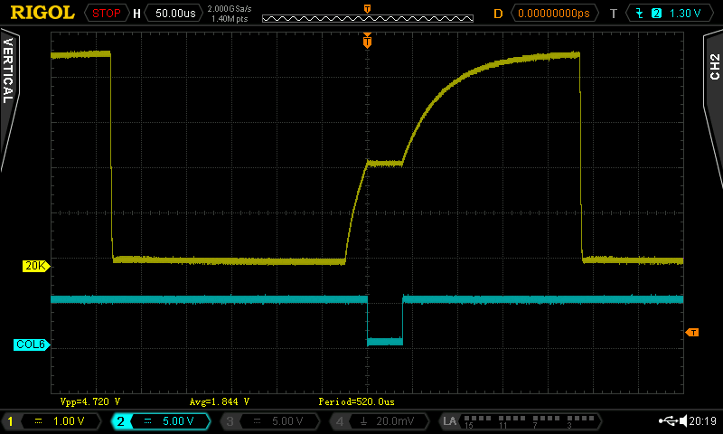
Influence of the keaboard scan (COL6) on the measurement of the POT**
The previous image shows that while COL6 is low, the capacitor does not charge => the line is flat while this happens. The keyboard scan is not synchronous to the measurement cycle, so the position of the flat line varies.
Of course the audio signal of the SID is an interesting waveform to probe. On boot, there is not anything to be heard, so I have used the SIDalyzer to set the waveform, volume etc.
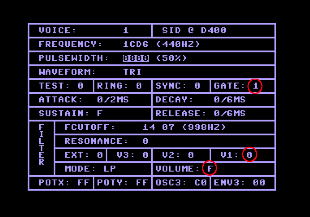
SIDalyzer setup
The volume needs to be set to maximum, the voice 1 should not be filtered and the waveform needs to be gated (=audible).
The SID output is U9, pin 27.
The settings:
Coupling = DC
Trigger= rising edge
Time = 2ms/DIV
Voltage = 1V/DIV
The SID output is U9, pin 27.
The settings:
Coupling = DC
Trigger= rising edge
Time = 2ms/DIV
Voltage = 1V/DIV

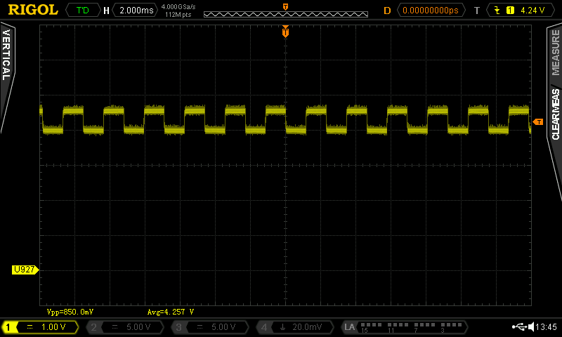
Triangle wave, 440Hz, maximum volume
The wave form shows, that there is quite a bit of an offset voltage (about 4.25V) and the amplitude of the audio signal is about 850mVpp.
Squarewave, 440Hz, maximum volume
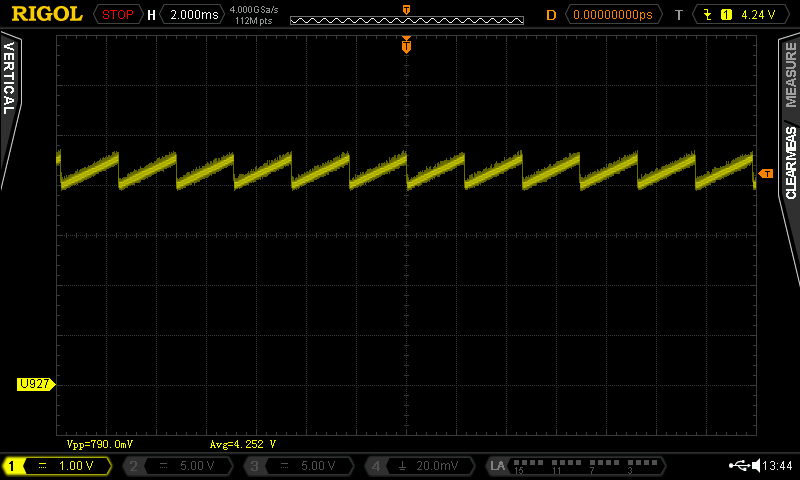
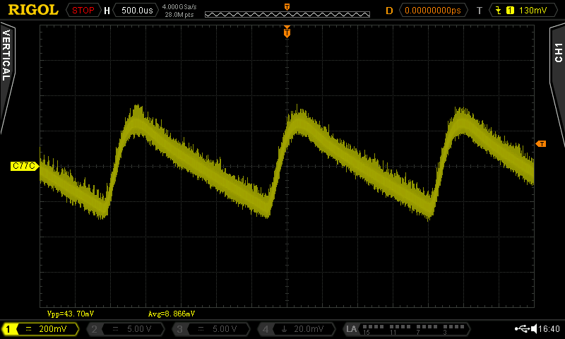
Sawtooth, 440Hz, maximum volume
The sawtooth signal is pretty hard to trigger in a way, that the waveform is steady. The problem is caused by the noise, that is contained in the output signal.
This requires a closer inspection.
Coupling = AC
Trigger= rising edge
Time = 500us/DIV
Voltage = 200mV/DIV
Sawtooth, 440Hz, AC coupling, 200mV/DIV
The inherent noise is clearly visible as a wide band. The SID output signal is not HiFi audio. That's for sure.
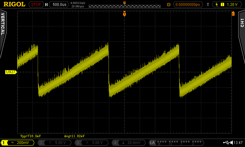
The transistor Q3 does noch change the signal a lot and the e-cap C77 is filtering out the DC offset. So finally, the audio output (at the DIN jack) looks like this:
Coupling = DC
Trigger= rising edge
Time = 500us/DIV
Voltage = 200mV/DIV
Sawtooth, 440Hz, DC coupling at C77 (cathode).
At the cathode of C77, which is the signal at the A/V DIN jack, the signal is DC free. The amplitude is about 670mVpp.
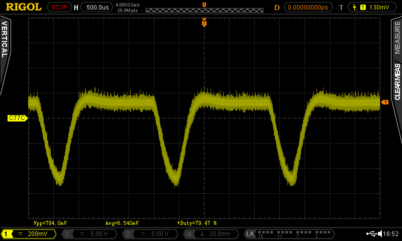
Now, let's switch on the filter! Or lets route the signal of voice 1 through the filter. The configuration is low pass, fc=998kHz.
Now, let's switch on the filter! Or lets route the signal of voice 1 through the filter. The configuration is low pass, fc=998kHz.
Sawtooth, 440Hz, DC coupling at C77, LP filter, fc=998Hz
Remarkable is, that the filter inverts the signal (the sawtooth is now backwards). The corners of the sawtooth are rounded, which is a result of the low pass filtering.
A square wave output signal with a pulse width (actually a duty cycle) set to 80% looks like this after C77:
A square wave output signal with a pulse width (actually a duty cycle) set to 80% looks like this after C77:
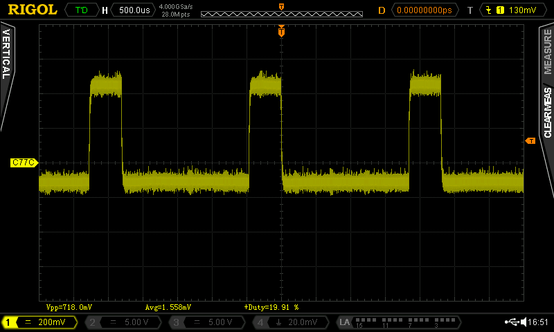
Squarewave, duty cycle 80%, DC coupling at C77 (cathode), no filter
This actually looks like a duty cycle of 20% ("on" for 20% of the time). Next, the low pass filter is switched on:
Squarewave, duty cycle 80%, DC coupling at C77 (cathode), LP filter (fc = 998Hz)
Again, the filter inverts the signal. Now, it really looks like 80% duty cycle (the scope measurement reads 79.47%). The corners are rounded due to teh low pass filtering.
Is the 6581 SID od earlier ASSYs any better (or worse) than the 8580 of ASSY250469?
Here is a screen shot of the audio output of a 6581:
Is the 6581 SID od earlier ASSYs any better (or worse) than the 8580 of ASSY250469?
Here is a screen shot of the audio output of a 6581:
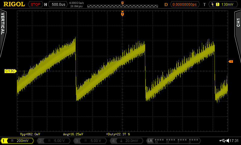
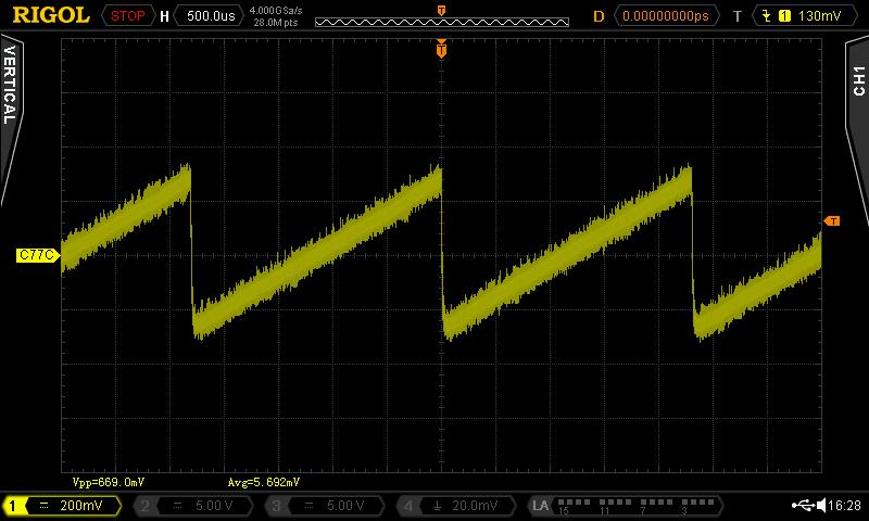
6581: Sawtooth at C13 (cathode)
In ASSY250425, C13 has the same function (filtering out the DC) like C77 in ASSY250469. It is clearly visible, that the ouput signal is about as noisy, maybe even worse.
The SNR (signal to noise ratio) is one criteria for good audio signals. It should be as high as possible. It is defines as
SNR = 20 log (SignalRMS/NoiseRMS)dB
An SNR of 80dB is a good one.
Measuring the SNR requires a special audio analyzer (as far as I know), like the Audio Precision. When I started working as a hardware developer, I could play with such a tool. I have made things with an SNR of 100dB and better.
The Fourier transformation is showing a spectrum of the measured signal. A perfect sine wave has only one peak in it's spectrum at the frequency of the sine wave. All other wave forms have harmonics, that are peaks of different heights at the multiples of the frequency of this waveform. What a decent scope can do is the Fast Fourier transformation (FFT) of waveforms. This method is "good enough".
A triangle wave is a bit like a sine wave. It has some harmonics, though. But their amplitude drops quickly.
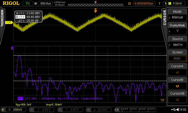
FFT (purple) of the triangle at the audio output (yellow)
Three harmonics are visible (the peaks of the purple curve at the left). Everything right from those peaks is mosty noise. The cursor is set to the level of the first peak.
Now, the output is muted. So, this is probably pretty close to the noise level.
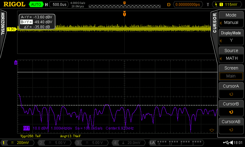
FFT of the muted output
The 2nd cursor is set to the amplitude of the noise spectrum. The difference is about 36dB. This value is not the SNR, it is much better.
Since the SNR is about RMS voltages, we could try measure those.

Triangle wave VRMS = 220mV
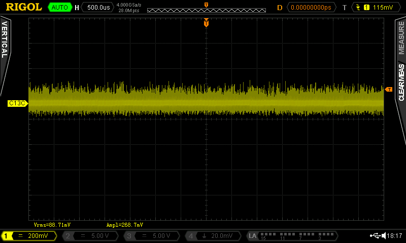
Muted output: VRMS = 89mV
The Triangle wave still contains the noise, the muted output might contain some traiangle wave, but we can caltulate it nevertheless:
20 log (220mV/89mV) dB = 7.86dB
The real SNR will be worse than 36dB (which is already bad) and maybe better, but close to 8dB.
Both is quite bad. So in case somebody starts ranting about certain SMPS power supplies that have a bad influence on the SID audio quality, just say "Rubbish!".