


A Beginner's Guide to PCB Layouting
Table of Content
1 Preface
2 The schematics
3 A good layout starts with good part libraries
4 The placement is essential
5 Routing
5.1 Preferred Directions, Vias
5.2 Supply Signals First
5.3 Copper Weight/Layer Thickness
5.4 Track Width/Distances
5.5 Layout Optimization
5.6 Ground Planes/Copper Pouring
5.7 Thermals
5.8 Markings and Silk Screens
6 SMD PCBs
6.1 Differences Between SMD and THT Layouts
6.2 Things to Keep in Mind/Issues
6.3 The Completed SMD Layout and Finishing
6.4 Fiducials
7 A Creepy Layout
8 Design rule check
9 Gerber Files
9.1 info.txt
9.2 Gerber Viewer (free)
9.3 Ordering PCBs
1 Preface
My name is Sven Petersen. I am an engineer and into professional electronic hardware development since 1995. I started as a hobbyist in 1979 and soon after that, I have made my first PCBs using a permanent marker on raw PCBs and ferric chloride… what a wonderful mess!
In my first job, all layouts were done by a PCB layouter, who was specialized on that. There was lots of time and communication required to enable him doing the layout. In my next job, I had to do the PCB layouts myself and I was not really great at it. Nobody told me, how to do it. It took a while to figure out the best practice for me.
While doing first layouts, I have experienced, that the more signals were already routed, the (exponentially!) harder it got to route the next tracks. That was, because I did not follow some basic rules! And this is, what I want to present here.
For the first layouts, I have used an auto-router. That was the (back then pretty bad) Eagle Auto-router. Then we had a pretty famous an expensive one: the Specctra auto router, which later became Cadence. Compared to the Eagle auto-router from end of the 1990s a really great product. But: Auto-routers need to be configured for each project and you can spend lots of time for that. It can be complicated.
I have usually spent quite some time to hand-optimize the layouts, that "dropped out" of the auto-router, because the customer had paid for a layout and not for an auto router result. After a year or so, I noticed, that I spend probably as much time for optimizing this kind of layout as I would need to do it completely manually. Now, I am so used to manual routing, that I wouldn’t go back to those auto-routers anymore.
Layouting is no witchcraft, you know.
Usually, it is not very hard when you follow some rules. I always wonder, that many other engineers like somebody else to do the layout for them (actually great, because this was part of my job). As a developer, you know the circuit, you have designed, very well and you should also know, what is important or needs some special treatment. Communication all this and finally checking the whole layout requires quite some time and will never be 100% effective.
Nowadays, I feel, that layouting is kind of meditation and I really enjoy this part of the projects.
This guide addresse the interested beginners of layouting. I do not want to promote any CAD software, here. I am using Eagle since 1997, the open Software KiCAD is widely used in the DIY scene.
2 The Schematics
The schematics, drawn in a CAD program, is not just lines on paper, but it is also the connection data of the circuit, that you have drawn. It contains the parts and their interconnects, when drawn properly.
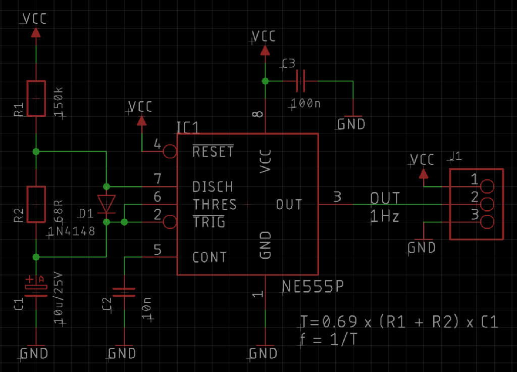
Figure 1: Schematics
It is important to connect the ends of the pins with “wires”, otherwise, they might look connected, but they are not connected. So, it is advised, that the grid and snap to grid stay switched on all the time. But I was a bit overhasty, because…
3 A Good Layout Starts With Good Part Libraries
Before you draw a schematic with a CAD tool, you need to have libraries with the symbols and footprints of the components, you will use for your project. Many people try to find one on the internet and even ask in some forum for a certain library. That is sure time consuming and you never know, what you will get. Usually, the symbols of those libraries are not the greatest and the footprint might not even be approved. I would recommend to make your own libraries.
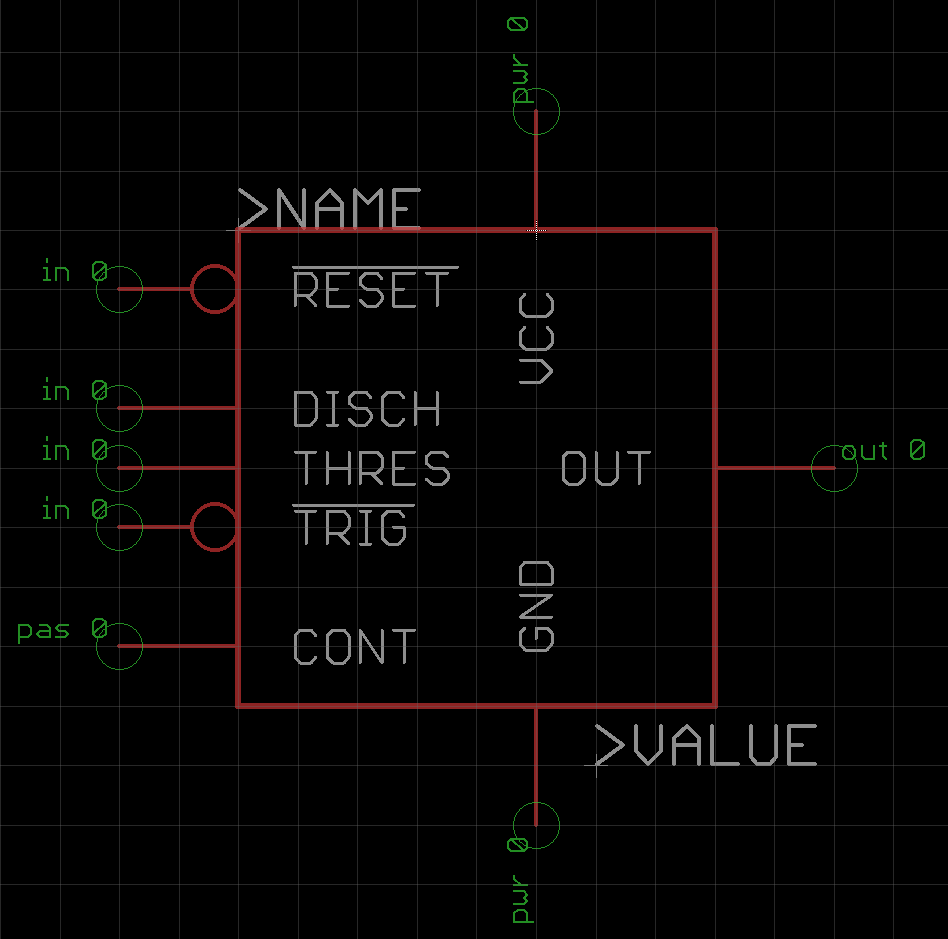
Figure 2: A schematic diagram symbol (for the NE555) in the library editor
It is well spent time to think about the schematic diagram symbol. Maybe it is good to use the same symbol like in the datasheet. Maybe it is not. It is recommended to group the pins, which will usually be connected (by wire or other components) or which belong together, like data bus pins. Creating a symbol, that resembled the pinout of the physical IC is not good. The “direction” of a pin should be correct. That can be in, out, pas(sive), power, etc. This might help to unveil failure.
It is important to stay in grid for the pins of symbols. Usually, that grid is 100mil/2.54mm. So, do not switch off "snap to grid" (or however it is called in your library editor).
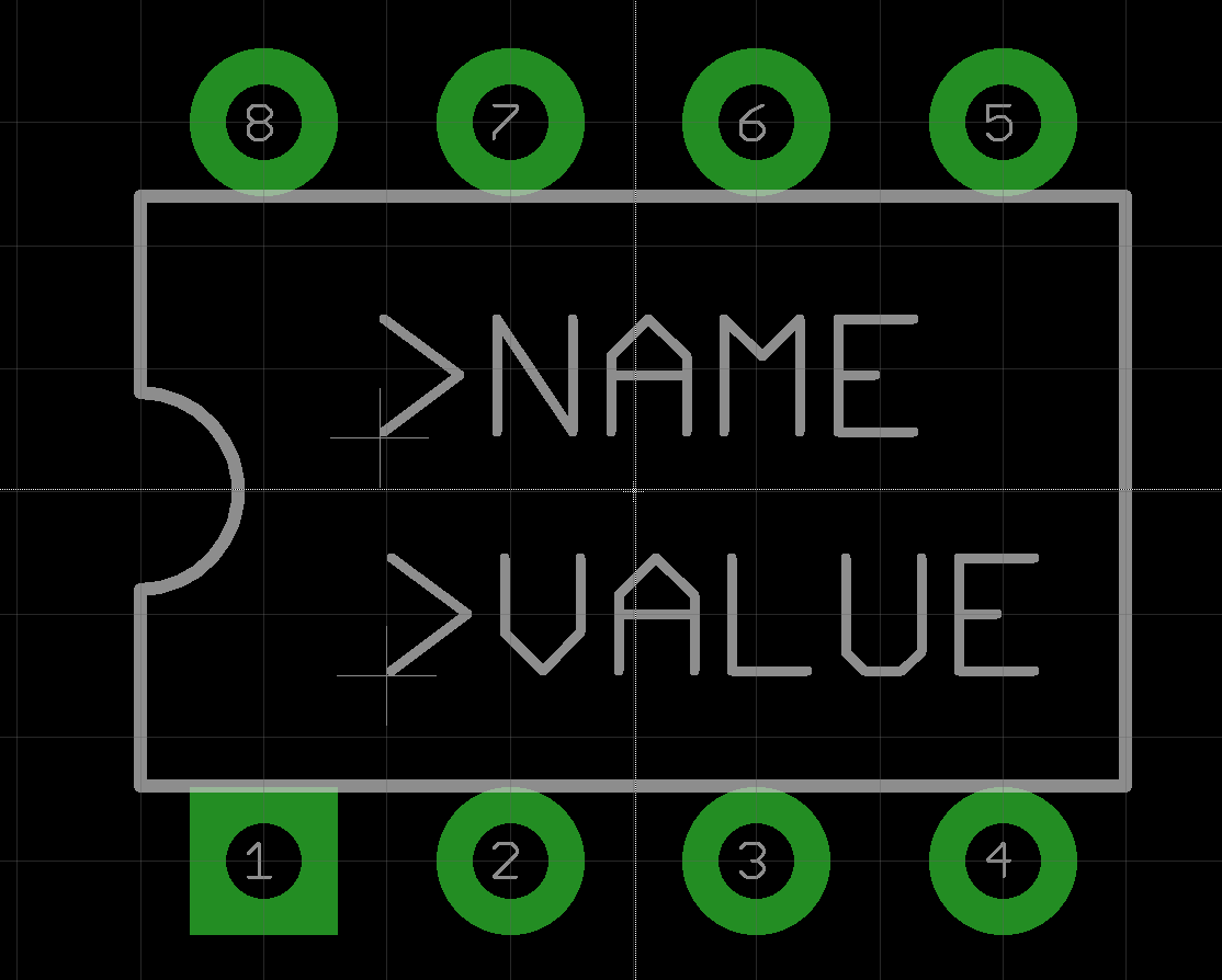
Figure 3: A DIP-08 case in the library editor
Many standard parts like DIP-08, 0805 or PLCC44 have decent footprints in the standard libraries of your CAD software, which you can copy and paste into your own libraries. It is quite practical, to have separate libraries for every manufacturer. This way, you can find those parts easily, when you want to use them in other projects or you can look up the library name in your schematic to find out the manufacturer later.
Look for footprint recommendations in the data sheets. Especially for through hole parts you have to have a suitable drill diameter for your pads. If there is none, calculate the diagonal of the pin (Pytagoras‘ a²+b²=c² is your friend) and add 0.2mm to get a suitable drill diameter.
Eagle can calculate the outer diameter of the pads automatically. It can of course be set manually. The copper around the drill is called an "annular ring" and it should not be narrower than 10 mil for pads and 8 mil for vias.
For surface mount parts, don’t make the pads too big. Just consider the tolerances in the data sheet for maximum with and length of the pads. The best is, to copy and paste from the standard libraries.
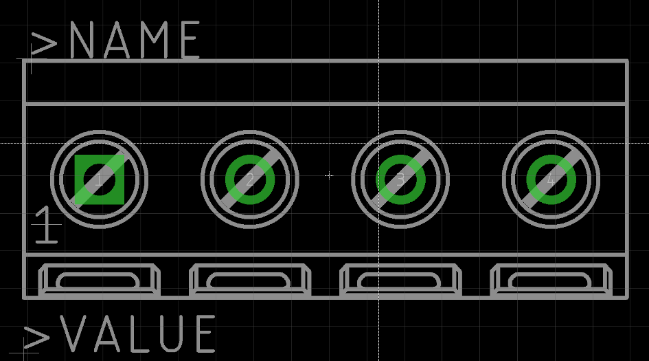
Figure 4: The footprint of a screw terminal connector
Draw the shape of the parts properly. You want the parts placed beside each other to fit into their place. If your footprint is too small, you might have conflicts. Also, the orientation should be obvious. The person, who has to assemble the boards later will ask you lots of questions, if that is not the case. Maybe you are this person and you cannot remember, what you have thought of, when drawing the footprints. A good footprint is useful and prevents trouble.
Depending on your ability when handling 3D data, there are 3D models of many parts (especially connectors) available from the manufacturers of the parts. I usually download these 3D models, made a DXF file from the top view and imported it into my (Eagle) libraries. This might sound a bit advanced (indeed, it is), so you can keep it in mind and try it, when you feel more comfortable with creating library parts. It definietly looks impressive.
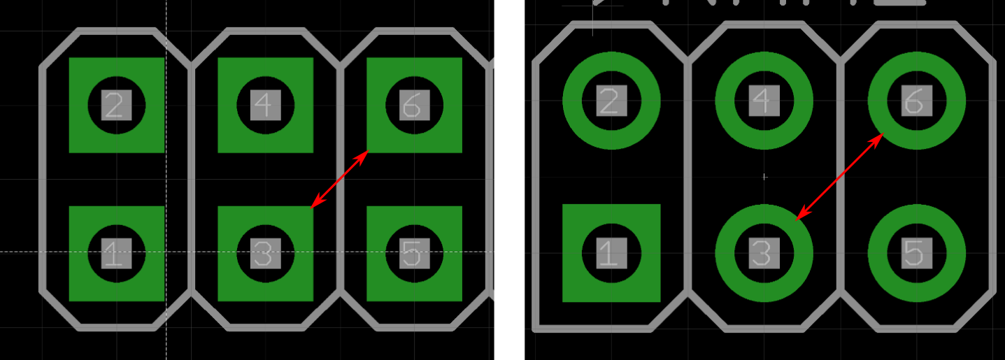
Figure 5: Square versus round pads
Do not use oval or square pads! They take more space than required and you rather use it for your layout. Let’s imagine, you have a connector with two rows. With round pads, you can easily get two traces through the space between two diagonally adjacent pins (Figure 5). With square pads, you only get one through there. A square pad for marking Pin 1 is quite handy, though.
Story time!!! Back in the past millenium, a colleague (who was the square pad advocate), had designed an adaptor board for a high voltage cable tester. I think, those high voltage test were carried out with 1000 volts. As you might know, electrical fields are highest on acute angles (that is where lightning strikes). The "pointy" 90° angles was good enough for some beautiful sparkover. No, square pads are not really great!
4 The Placement Is Essential
After the schematic is drawn, it is required to create a board file. This is usually pretty easy. Just click an icon and you will get to the PCB editor.
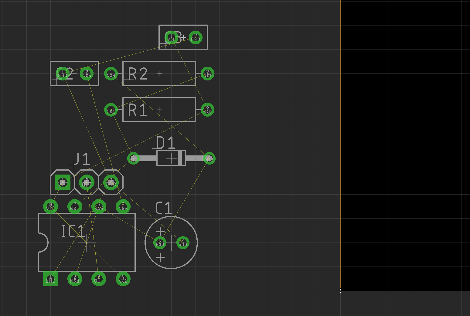
Figure 6: Initial state of a PCB, that was just created from the schematics
Initially, the parts are placed outside a PCB of a standard size (Eagle: 100mm x 160mm). These placements usually do not make any sense (Figure 6). The thin lines between the pins are called "air wires" aka rubber bands (which resembles the "elasticity" of them).
They are the connections, that were created by drawing the schematics. Making a layout is all about creating proper copper tracks on the top and bottom layers (or maybe some inner layers) from those air wires. But first, the parts have to be placed in a meaningful way.
The time spent for a decent placement is usually not wasted. There are several criteria, that have to be met and some contradict each other, sometimes.
Usually, there are some connectors, that may have to be on one edge of the board or an electrolytic capacitor should not be too close to a heat sink, since they tend to dry out and start to lose their capacity. Sometimes, the tracks have to be as short as possible, etc.
The other components should be placed in a way, that the layout is least complicated. In total, the tracks should be (nearly) short as possible. Especially in analog circuits with many discrete parts like resistors, capacitors, diodes, transistors, etc. the components, which are close together on the schematics are likely to be close together on the PCB, too. Placing them like this is a good start point, that can be optimized later.
In the CAD software “Eagle”, the air wires do not automatically snap to the next closest connection, when moving around the parts. You have to refresh the air wires by clicking the “ratsnest” icon. This will be required every now and then. The air wires will then snap to the shortest distance again, so you can check, if your placement has the effect, you intended it to have. Other software packages usually have a similar function.
Figure 7 shows a good placement. It might not be possible to determine the perfect placement with this method. It will show its quality, while routing the tracks. Maybe, it will be required to (slightly) move around the components, while doing the layout.
For more complex circuits, it might be a good idea to place the components in groups first and then move those groups to the board in a second step. After that the placements can be modified further. Sometimes, there are similar groups in a circuit, like several identical input channels that are equal. It makes sense to also place them equally.
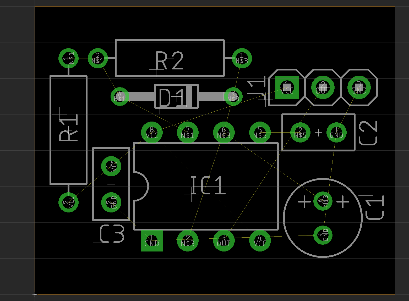
Figure 7: Placement of the components
5 Routing
Now, it is time to start routing the rubber band! But… hold it… we have to thing about something prior to that! It is a good practice to follow preferred directions on each layer of the board.
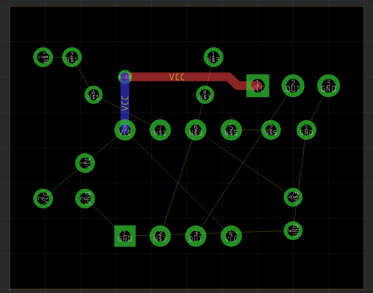
Figure 8: The first track
5.1 Preferred Directions, Vias
For a through hole layout, this is a choice, that usually can be done easily. Just pick one. Let’s say “Top horizontal, bottom vertical.” It is only important, that you follow this while routing.
The track in Figure 8 might look stupid. It would be possible to route directly on one layer, not having to have a “via”. A via is a through hole connection of tracks on two different layers. It is plated through like an ordinary solder pad. But the diameter is smaller. 20 years ago, 0.6mm/24mil vias were standard. In 2020, I would recommend 0.35mm maybe 0.4mm, if the current allows such a small via. For higher currents (like in a power supply) I still use 0.6mm maybe even more than one via.
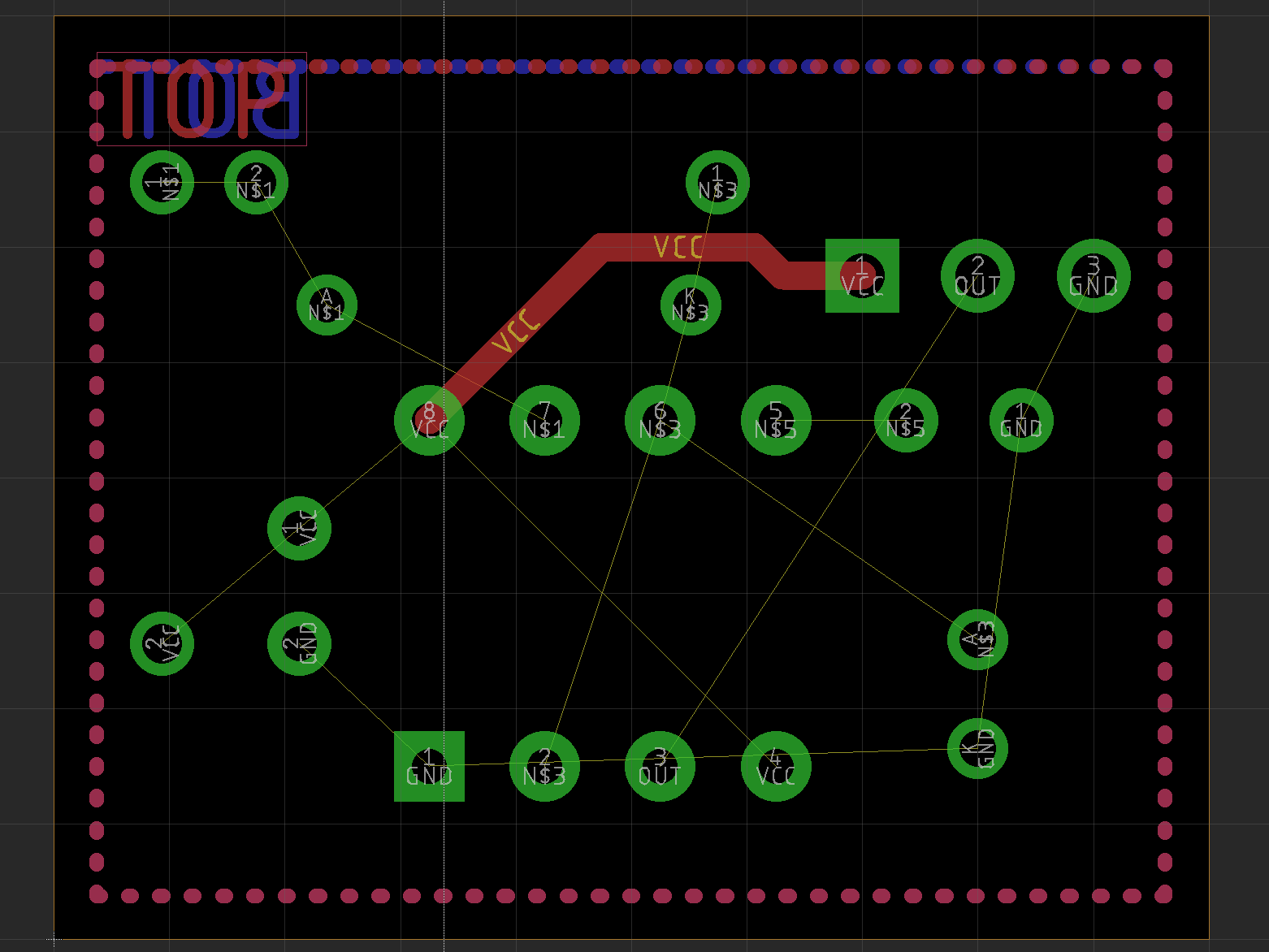
Figure 9: Don't do this! Direct routing without following the preferred directions
The track in Figure 9 might look smarter, but it does not follow the previously chosen preferred directions. Doing so will cause the layout to get exponentially more difficult, the more rubber bands are routed! A layout with preferred directions might get a bit harder on the way, but not much harder. And in case the prototype requires a revision (which happens quite often), it is not a really big deal to modify the layout.
5.2 Supply Signals First
It is a good practice to route the supply voltage(s) and ground(s) with wider tracks. Both, especially the grounds should be low impedance. The ground is the reference and a significant voltage drop on ground might result in malfunction. This is the reason, why it is a good practice to route GND and VCC (or other power potentials) prior to the rest of the tracks. This is shown in Figure 10.
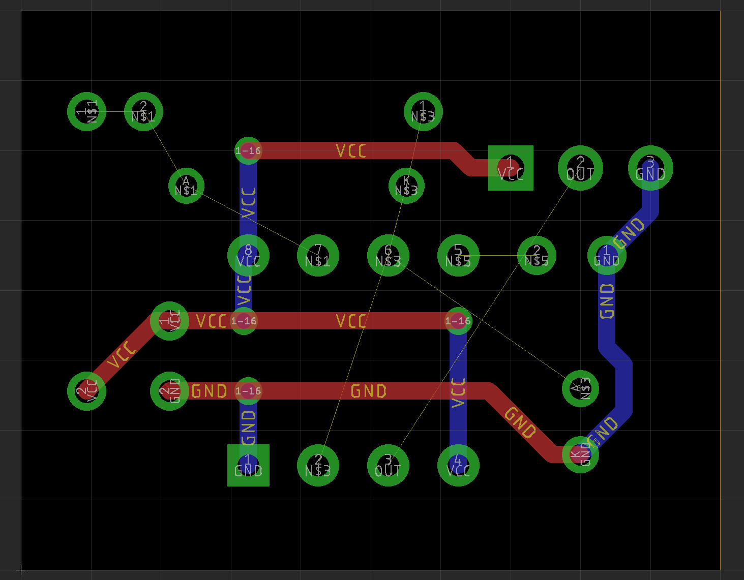
Figure 10: GND and VCC routed first
5.3 Copper Weight/Layer Thickness
For “normal” circuits, like “something digital, some analog ICs” things, it is ok to use a width of 24mil/0.6mm for VCC and GND. Higher currents will require wider tracks or even a thicker copper layer. Average PCBs have 35µm (1oz) copper layers. Higher currents might require 70µm (2oz), this is the choice you have with most “cheap prototype PCB manufacturers from China”. For high current layouts, 105µm (up to 400µm) copper is possible. But this will usually not occur in DIY projects. For this purpose, 35µm copper are recommended.
The supply voltage tracks in Figure 10 are routed following the preferred directions chosen before.
5.4 Track Width/Distances
Now, only the “other signals” are left and require routing. Nowadays, 6mil tracks (and 6mil distance) are possible with the said prototype manufacturers. Personally, I stay with wider tracks, if possible. So, my choice is 8mil, 10mil or even 12mil tracks (12 mil was the standard in the late 1990s). It just reduces the likelihood of failure (slightly).
1 mil is 1/1000 of an inch = 0.0254 mm
The remaining signals are all routed following the preferred directions. The result is already a working PCB layout. But careful! A design rule check is still required to prove, there are no overlaps or that the tracks are too close together.
The standard for PCB layouts is the IPC-2221. Here is an excerpt regarding the maximum current for the track width for 35µm/1 oz copper (this is, what you will usually use).
The temperature rise means, if your PCB lives in a 40°C environment, the track temperature will be 10°C higher (=50°C) or 20°C higher (= 60°C).
Find more tables here.
Sometimes there are safety requirements for the track distances. I do not encourage you to do layouts incorporating high/mains voltage. Those require wider distances between each other for safety reasons. For 230VAC, I use distances of 5mm between L(ife) and N(neutral) and PE. And more than 6mm to the low voltage part. It depends on many things, even the desired maximum height above sea level and of course the degree of contamination. That is engineer's stuff!
5.5 Layout optimization
Finally, all signals have to be routed, taking care the required width and distances and of course the preferred directions..
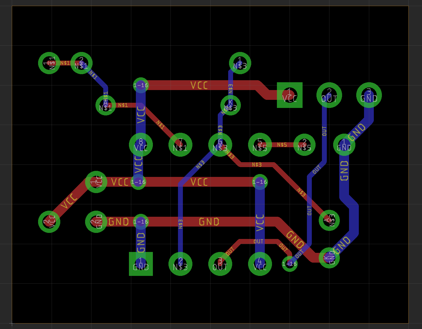
Figure 11: All signals routed!
Before declaring the layout to be finished, some cosmetics should be done. First, the tracks can be optimized a bit. That means making them shorter by using more diagonal directions (Figure 12).
Figure 12: Optimized layout
There is not much difference of the optimized layout. It is a pretty simple circuit anyways. Using the diagonals will free some space, that can be used for other tracks being shorter, too. Mainly the VCC tracks have been modified, here. One track (the topmost VCC path) was ripped up and routed again.
In technology, it is required to be able to dump old ideas or work for creating something better. PCB layouting is a good thing for practicing this philosophy. Since I enjoy this work, it is not even hard for me. It is a bit like cross word or sudoku, but the result will be of great use.
5.6 Ground Planes/Copper Pouring
Like mentioned before, especially the ground (GND) potential should be as low impedance as possible. It is the reference for all signals in the circuit. If it is “moving” (due to voltage drop), everything is less determined. It is not completely unlikely, that problems can result from GND problems.
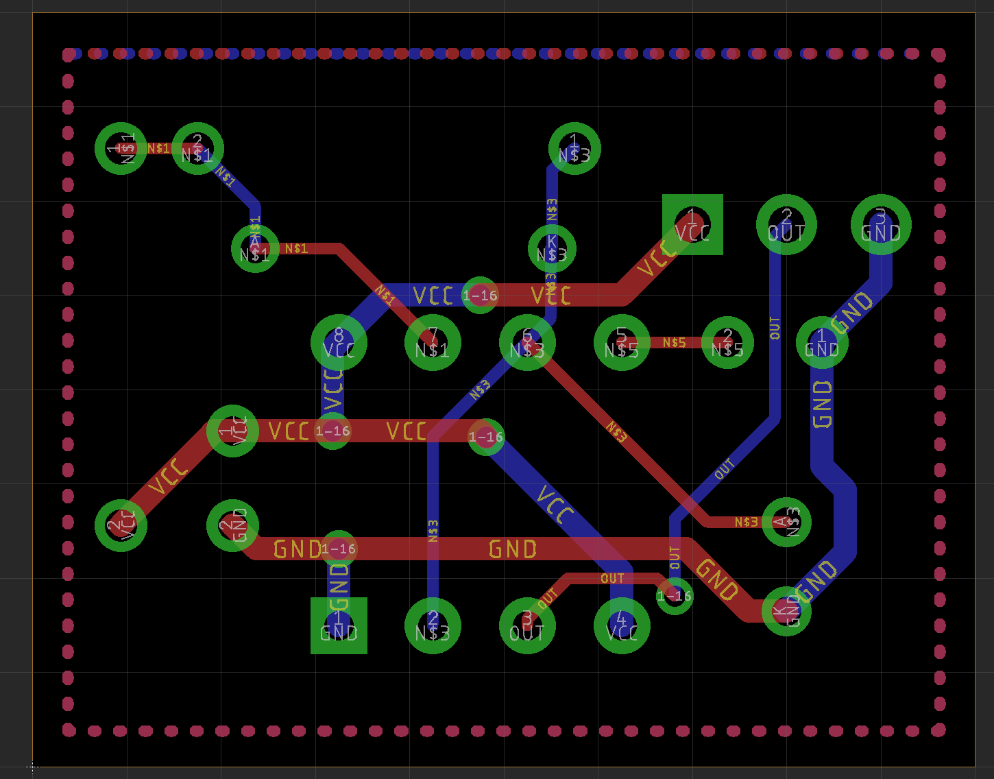
Figure 13: Layout with ground "polygons"
Hence, it is best practice to add ground planes to the PCB. Actually, it is a copper pouring, which I am talking about. There are no extra copper layers required. The desired outlines of the pouring are drawn as polygons, which are assigned to the GND signal. The possible infill will be calculated automatically be the software. The infills might look complex, but it is no work, that has to be done! The computer does it for you.
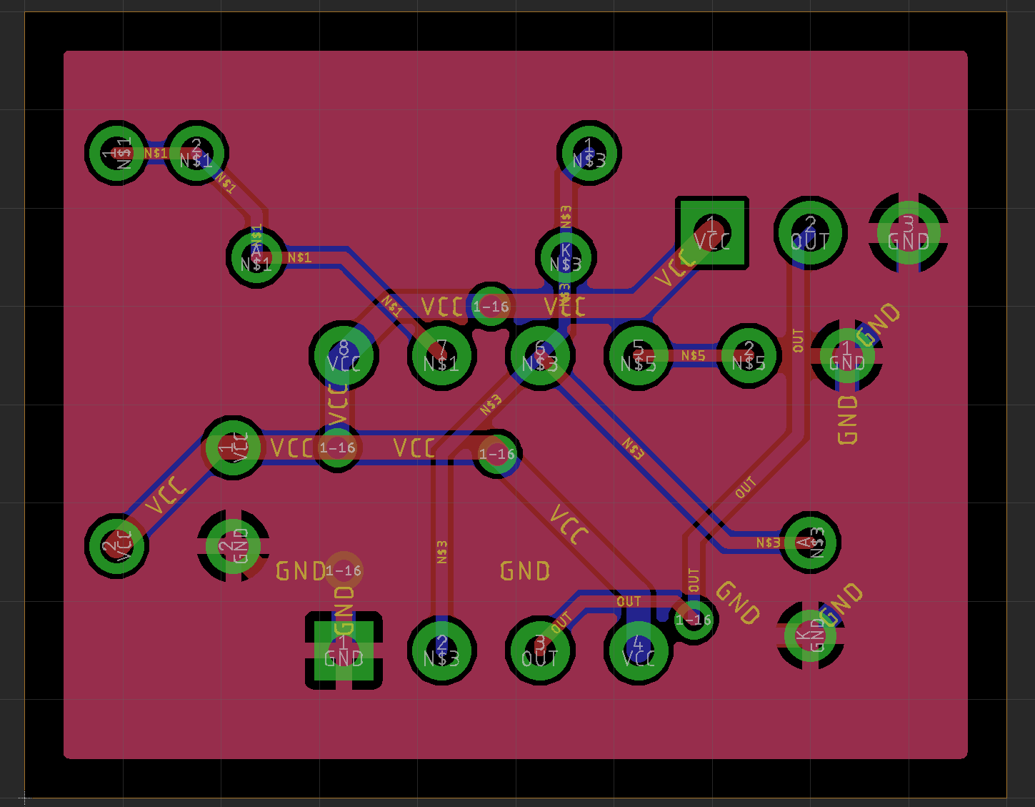
Figure 14: PCB with copper pouring
The copper pouring is calculated, so that a minimum distance to all other signals is met. Other than having a low impedance reference potential (aka ground) the copper infill helps to keep the (electro-magnetic) emissions low. I never had issues with emissions of my boards in EMI compliance testing.
Story time!!! I once helped a customer to get through the mandatory EMI compliance test. He had a company logo, that incorporated a line and that logo was on the top copper layer of the PCB. Of course, the line was not connected to anything. First there were problems with the emitted fields. It took a bit to track that down to something. It was this line, which worked as an RF transmitter (it had the perfect length for the spectral frequency, that was above the limit). After covering it with a copper tape, the problems were gone.
5.7 Thermals
The GND pads are connected to the copper infill with a “cross”. This is called a thermal. Planes are hard to solder, because the heat seems to escape through the mass of copper, that is connected. Copper is a great heat conductor. To keep the problems as small as possible, those thermals are generated. The GND pads are still a bit harder to solder than normal pads, but it would be much harder to solder them without those thermals.
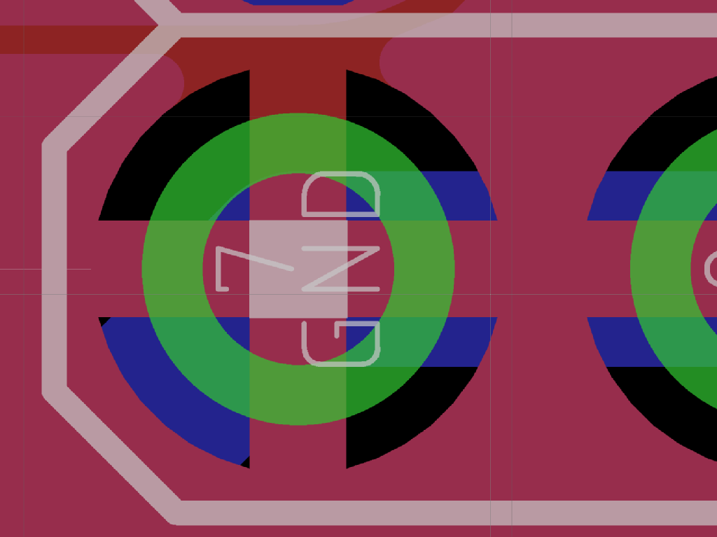
A thermal
Story time!!! In a very high current design (up to 200A!), I have disabled those thermals. Even for professional assembly houses with wave soldering machines, the pads have to be inspected carefully for proper solder joints and might require some rework. Sorry for that, but the design requires it. So, use thermals, whenever possible.
5.8 Markings and Silk Screens
With through hole PCBs, it is not always obvious at first glance, which side is top and which is bottom. So, it is best practice to mark the sides.
This is should be done in a free space somewhere in the copper, like in the top left corner in Figure 15).
For industrial purposes, the “silk screen” (which is the drawing of the placement on top and maybe bottom of the PCB) is usually not required. Those boards are installed by experts, they know, what they are doing without this print.
The prototype PCB manufacturers offer top and bottom silk screens for the same price, so it is a good idea to make use of them and add as much information as possible.
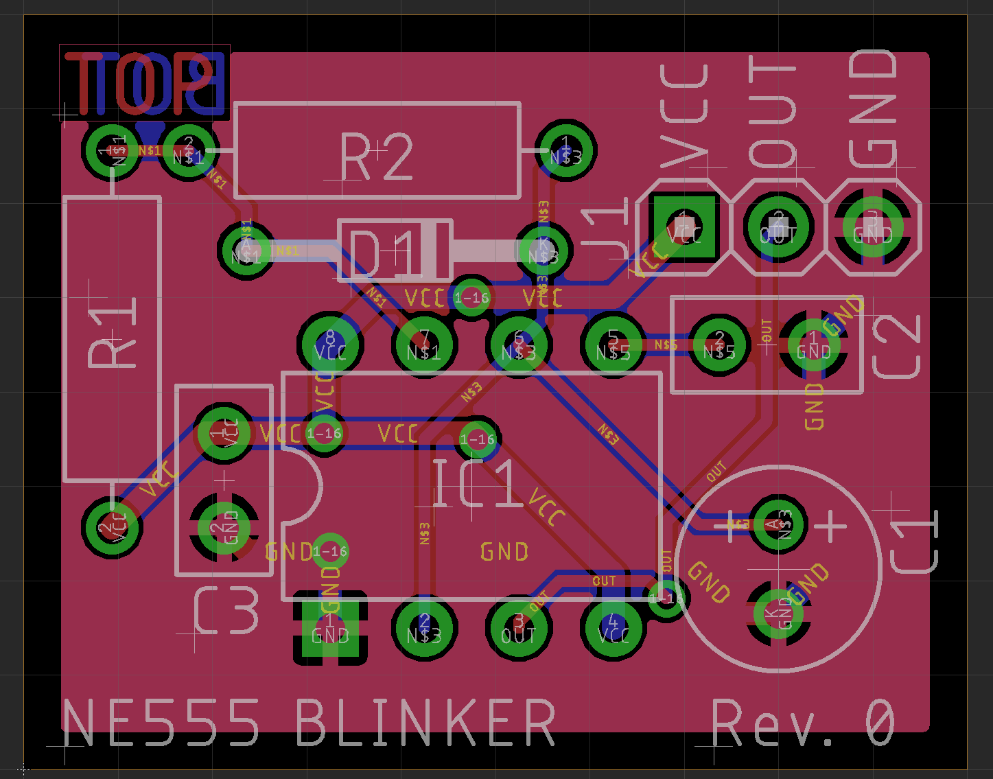
Figure 15: Finished layout
The reference designators (Names of the components), like C1, C2, R1 etc. should not be placed above pads. This way, they are not visible and of no use. They need to be moved to a space close to the components, so it is clearly visible, which component they name. Spend some thoughts on it. When the PCBs arrive, you will not remember all the names or maybe somebody else will want to build your circuit, too and they should easily know, which part is placed where.
For some time, I am also into designing open hardware (sharing is caring). The difference to industrial designs, which I am doing for 25 years, now, is in the documentation and of course the maximum of information, that is put on the silk screen, since those projects do not address the professionals, but the tinkerers at home. This is the reason for the “VCC, OUT, GND” marking at the connector J1.
It is required to be able to identify the boards, easily. After many hobby projects, you will have a box full of PCBs. It should be obvious, which project they belong to and also, which revision they are. My first prototypes are “Rev. 0” (we tech people start counting from zero, right?). The next PCB revision will be “Rev. 1”. I count it with whole numbers. There are no half revisions. Ok, this is my philosophy, others can do it in a different way. The only mistake is not adding a revision number to a PCB. For designs without a silk screen I add a project number and revision like “ppp/nn” somewhere in the copper.
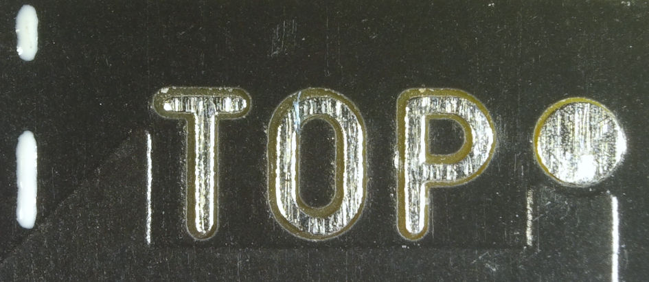
TOP marking and fiducial on a real PCB (free of solder stop mask)
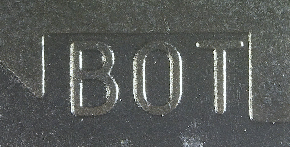
Bottom marking on PCB
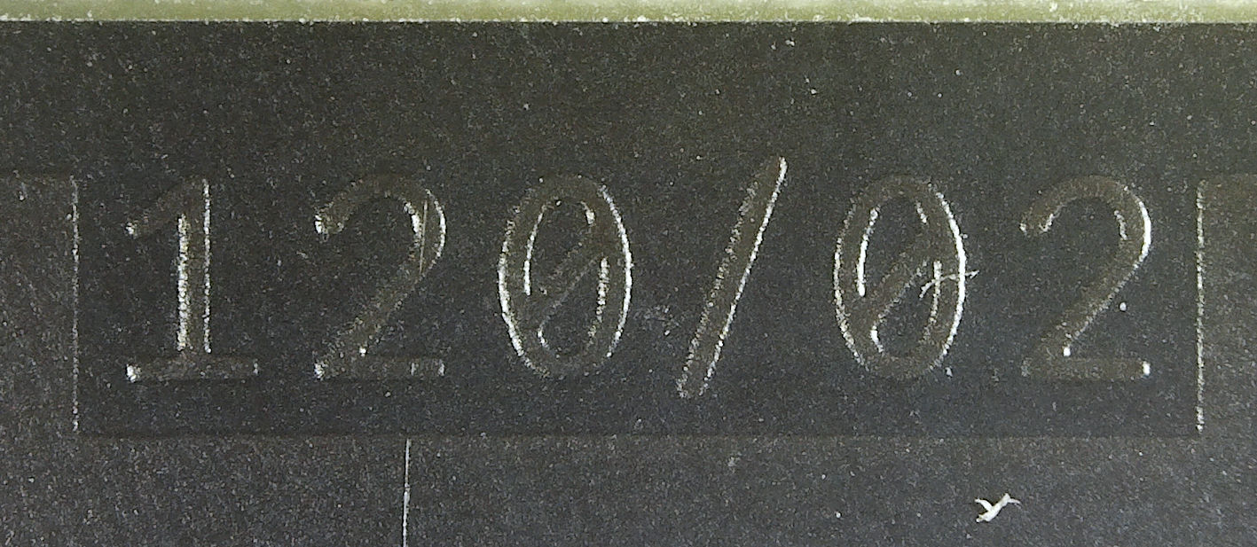
Project number and revision for identification purposes
6 SMD PCBs
SMD means “surface mount device”. Nowadays, those are the preferred parts for industrial assembly. The advantages are pretty obvious:
● SMD components can be placed by a machine
● SMD components are smaller
● The solder is screen printed with a stencil prior to the placement of the parts
● The soldering is happening in a reflow or vapor phase oven
As a result, many “advanced parts” are not offered as through hole parts anymore. The hobbyist sometimes has no other choice than using SMD parts for his projects.
The soldering of many SMD parts with a small solder tip should not be a problem. 0805 chip resistors and SO ICs (1.27mm pitch) can be accomplished at home, no stencil for solder paste or hot air soldering stations are required for this. There are plenty tutorials about SMD soldering on Youtube.
6.1 Differences Between SMD and THT Layouts
So, what is different with SMD layouts? Through hole footprints offer many free vias (the through hole pads). More (space consuming) vias might be required for a layer change while routing the tracks. This results in the need of determining the preferred direction prior to the placement. Actually, it means to also keep a preferred IC orientation. The two or three pin chip resistors, diodes or transistors are less critical. But in general, they should be placed in a way, that they do not block routing tracks from an IC to the outside.
6.2 Things to Keep in Mind/Issues
There are a few possible issues, that apply to all layouts, but the likelihood, that they happen in SMD layouts is higher than with THT layouts. THT??? Through hole technology, the “normal” stuff!
One issue are acute angles.
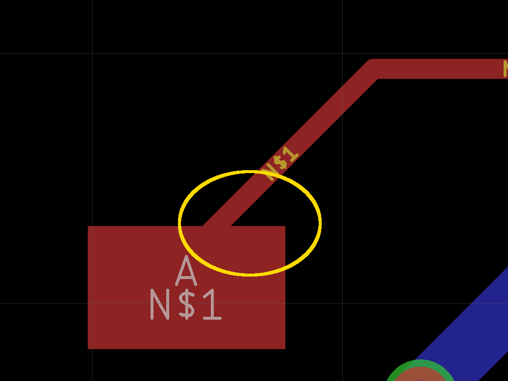
Figure 16: a 45° angle in an SMD layout
Acute angles have two disadvantages:
● The (thin) track is likely to break here. Acute angles are tolerating tension less than 90° angles.
● Residues of the acid from etching the board can stay there, which leads to destruction over a longer period of time.
The cure: Exit tracks vertically from SMD pads.
Another issue is caused by vias, which are too close to SMD pads. Especially, when the vias are not tented (covered by the solder stop mask), may “suck in” the solder from the adjacent SMD pad. This leads to problems while production.
The cure: The openings in the (automatically generated) solder stop mask must not overlap.
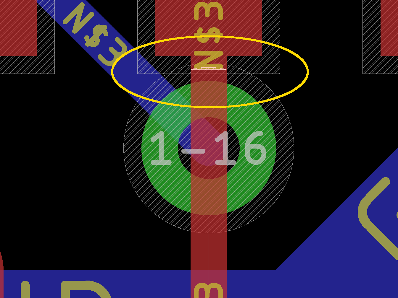
Figure 17: The via is too close to the SMD pad
Eagle is showing distance problems like shown in Figure 17 when they happen. A small area near the N of N$3 is crosshatched here.
6.3 The Completed SMD Layout and Finishing
The completed SMD layout is significantly smaller than the THT layout of the same circuit. It is the NE555 blinker again.
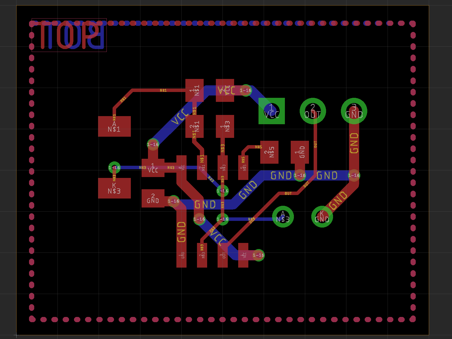
Figure 18: SMD layout after routing and optimization
For the optimization, the same rules/processes apply like for THT layouts.
While the THT layout required 3 vias, the SMD layout requires 8 vias. It might be an advantage to choose vias with 0.35mm drill.
The orientation of the SMD NE555 is resulting in the preferred directions: top vertical, bottom horizontal. There are some violations of those preferred directions. The signal N$1 (top/left) moves horizontally on the top layer. Do not start like this. After the optimization, it is ok. This violation saves two vias.
A good silk screen is a bit harder on SMD PCBs. Especially the chip resistors and capacitors are too small to contain the complete designator (name). Those have to be placed outside the component and like before, must not be placed over pads or not tented vias. They will not be readable otherwise.
6.4 Fiducials
For machine assembly of SMD boards, reference markers are required. The technical term is fiducials. A good choice is a 1mm circle in copper, which is free of solder mask.
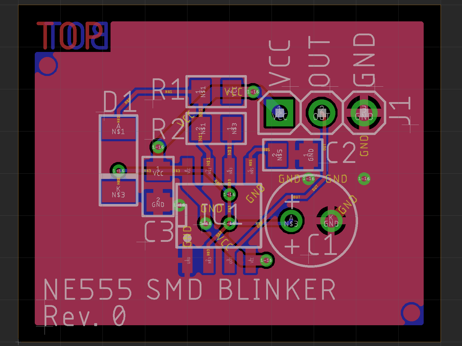
Figure 19: A fiducial/SMD reference mark
The SMD assembly machines reference the boards with a camera. The light structure of the fiducial can be found easily.
Bigger fine pitch ICs should also have two fiducials somewhere close to them.
While my job as hardware developer, the preferred shape and size of the fiducials have changed a couple of times. They have always been copper structures free of solder mask. There were 3mm circles, 3mm crosses, 1mm diamonds and finally 1mm circles.
They do not need to be positioned precisely on the diagonals, usually they are placed near the diagonal corners. All SMD parts should be within the rectangle that they span.
Note: fiducials on the silk screen are not a good idea. The silk screen is way less precise than the copper layers.
7 A Creepy Layout
Deep in the archives, I have found a pretty creepy auto-router layout from the last millenium, which I would like to discuss. I think, I had already used the famous SPECCTRA auto-router for it.
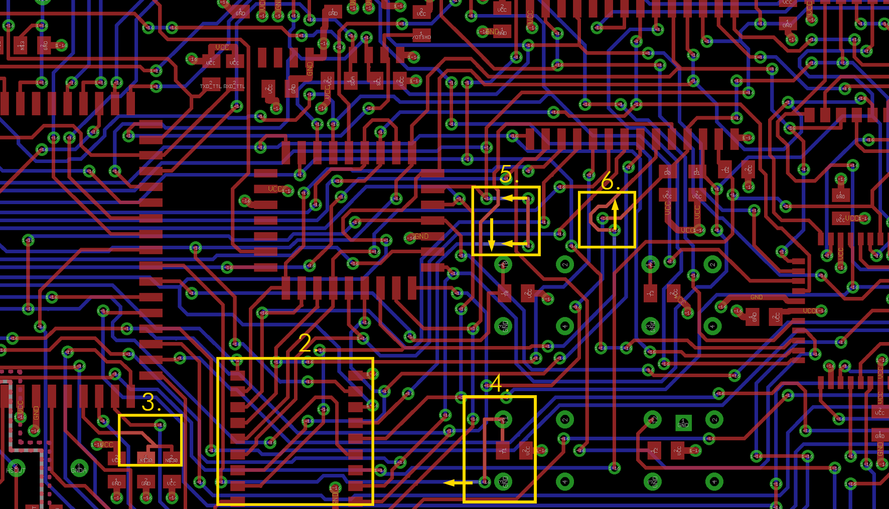
Figure 20: The bad and creepy layout
There are plenty problems in this layout. I will not mention all of them. This way a four layer board. The inner layers mainly consist of ground and supply voltage polygones. The top layer is red, the bottom layer is blue.
1. The fundamental problem in the layout is the lack of preferred directions on the top layer. It is a bit like the bottom layer was horizontal routing, but it is pretty mixed. Most of the other problems are a result of this Adding one more signal/copper track requires a lot of things, that need to be moved. Routing more signals gets exponentially harder. Rev. 0 of this PCB worked. I only had to have a Rev. 1, because one part became obsolete pretty early in the project life.
2. This IC is oriented in the wrong direction (vertically). Other SO ICs (top area) were oriented horizontally. That would also fit to the "most signals on the bottom are somehow horizaontal.
3. An acute angle. If the PCB breaks, it will probably break at an acute angle. There are several
4. The red track that goes up and then right is, what I would like to mention. This signal is longer than required. if the via (at the bottom of the frame) would be far more left, this could be a 45° track on the to layer would save a bit of length. Also the track then goes down to a chip resistor. It can be made shorter. Shorter tracks and less vias are a way to have more space for other tracks.
5. At the bottom of the frame, there is a horizontal blue track, which then changes layers at the right side or the frame, going up (red) the changes the layer (blue) ending in a via. This structure is too long again, and one via could be saved, if the 45° track below the last via would be oved down. It would be space for a via there, a vertical red track, that would directly connect to the last via. The complete structure right of it could be replaced this way.
6. Look at the vias. There is a red track, that forms a C around the via. This is humbug! if the right via would be above the red horiziontal part of the track, the C would not be required.
8 Design rule check
A design rule check after finishing the layout is absolutely mandatory. It includes the check for required distances and widths, also overlaps are shown.
I would recommend to set up the check for distances to 6 mil and for width, too. The minimum drill can be set to 0.3mm. Those are parameters, that the prototype manufacturers can handle.
Since the design rule check depends on the CAD software, I cannot include more details about it. It is also important, to check for left over unrouted air wires. The modern Eagle does it, many years ago, it was required to do a ratsnets and check for the number of air wires left, this way.
9 Gerber Files
Usually the PCB manufacturers do not accept the CAD design files (there are some). After the layout is finished and checked, Gerber files have to be generated.
The Gerber files consist of plotting commands for photo-plotters, which are standardized. Those photo-plotters “draw” the films used for the PCB production. There is one film per layer, so there is one Gerber file per layer. The preferred Gerber format is RS-274X. There are more advanced data formats, like ODB++, which get slowly established in PCB production, but not every CAD software is capable of them and as of 2020, Gerber is still pretty popular.
The drill files are created in a different format: Excellon is a good choice for it. A normal board is drilled twice. One before plating through, once after plating through. Holes, which are plated through, are connection the copper layers with a conductive plating of the walls of the holes. THT solder pads and vias are typically plated through. Other holes, like mounting holes or key holes (for parts and connectors) are not (necessarily) plated through. There are two drill files:
● Plated through holes
● Non-plated through holes
It can happen, that the latter file does not contain holes, since this kind of hole is not present in every design.
9.1 info.txt
Back to the Gerber files. Those have usually different endings, the file extensions. They are no standard, because different CAD software have different name the Gerber files differently. This is no problem, since the PCB manufacturers know how to handle them. It is a good practice to include a text file with information about the PCB and the naming. It is not mandatory, though.
My info.txt looks like this:
Board: <name>
Rev.: <rev>
Files:
======
All Gerber files are generated in extended gerber format (RS274X)
*.TOP : Film top copper
*.BOT : -"- bottom copper
*.STC : -"- top solder mask
*.STS : -"- bottom solder mask
*.PLC : -"- silk screen top
*.PLS : -"- silk screen bottom
*.CRC : -"- cream top
*.DK : Drills plated Through (Excellon)
*.NDK : Drills not plated Through (Excellon)
*.OUT : Board outline
Board Size:
===========
Length : 65.25 mm
Width : 56.0 mm
Thickness : 1.6 mm
Material : FR 4
Copper : 35 um
Surface : HASL
Remarks:
========
width > 6mil
distance >= 6 mil
drill >= 0.35mm
All files (Gerber, Excellon, info.txt) are packed in one ZIP file, it is a good practice to include the project name and the revision in the file name. To prevent any trouble, I counter check the files in the directory and from the info.txt one by one.
Story time!!! Many years ago, I accidentally forgot to include the Gerber files for the inner layers of a PCB in that kind of ZIP file. 100 PCBs produced, 100 PCBs assembled and none of them showed any sign of function. What a mess!!! The best about mistakes is, that you don’t have to repeat them.
9.2 Gerber Viewer (free)
Also, it is highly recommended to use a (free) Gerber viewer to check the Gerber data for plausibility. It is not testing every copper trace, it is just having a look at each Gerber file and considering, if the shown image is reminding you of the specific layer. No detail work required.
The free Gerber Viewer of my choice is the Pentalogix ViewMate.
9.3 Ordering PCBs
Now, your Gerber files are ready for ordering and upload. I am experienced with the prototype PCB manufacturers
● allpcb.com
● jlcpcb.com
● pcbway.com
● multi-cb
● Beta Layout
● Aisler
and others. The order does not show my preference.
Usually, it is pretty simple to order PCBs from them. 10 PCBs smaller than 100mm x 100mm are about US$5. The postage is the main factor. The price mainly depends on the shipment choice. The faster, the more expensive. A plain green PCB might be produced within one day, transport by DHL express takes another 2 or 3 days. So, the PCBs will be delivered within four days. Customs might take an additional day.